Memory control device

a memory control and memory technology, applied in the direction of memory adressing/allocation/relocation, digital computers, instruments, etc., can solve the problems of difficult to employ interleave-access methods, difficult become extremely complicated to achieve low-latency memory access with high throughput, improve bus utilization efficiency, and reduce read/write time.

Inactive Publication Date: 2010-04-27
LONGITUDE SEMICON S A R L
View PDF6 Cites 48 Cited by
  • Summary
  • Abstract
  • Description
  • Claims
  • Application Information

AI Technical Summary

Benefits of technology

[0015]Therefore, a memory-control device having simple construction and that is capable of increasing the bus utilization efficiency and making it possible for low-latency memory access with high throughput has been desired, however, it is difficult to accomplish this with the prior art.
[0016]In the light of the aforementioned problem, the present inventor thought that aiming at high-throughput low-latency memory access even on one bus would be good for overall efficiency. Therefore the present inventor has invented a memory-control device that improves the address / data communication efficiency when a plurality of ranks or modules are mounted on one bus.
[0031]With the present invention, commands and data flow continuously over the main memory bus, and it is possible to dramatically improve the bus utilization efficiency. The first reason for this is that it is not necessary to take into consideration the actual memory access latency for instructions issued by the memory-management unit. The second reason is that the time difference of usage of the data bus used for read instructions and write instructions is utilized, and instructions are rearranged with read instructions having priority. The third reason is that the rank-management unit and every memory rank are independent, and different instructions can be executed in parallel in the respective memory ranks, and rank interleave is performed according to an address-conversion table, so the clock related to address specified delay or pre-charge etc. is hidden, making it possible to perform data input / output at high speed.
[0032]Moreover, with this invention, by using read pre-fetch and an ACT instruction with data, it is possible to reduce the read / write time. The reason for that is that a one-word portion of the address continuing after a read instruction that was given to the command decoder is pre-fetched by the data buffer, and when it matches the next read instruction, it is possible to perform output at high speed. Also, data of a write instruction in the data buffer is constantly monitored, so data is saved and written in a memory rank even when data is output from an ACT instruction that is one clock preceding to the write instruction.

Problems solved by technology

In the interleave-access method, the amount of wiring for the address and data bus more than doubles, so the physical mounting space, such as the number of package terminals and board area, and the cost increases.
These mounting restrictions are particularly undesirable in a notebook PC in which there is a need to conserve space, or in an embedded system, so in many cases it is difficult to employ an interleave-access method.
Therefore, it becomes extremely complicated to achieve low-latency memory access with high throughput.
Also, there is a problem unique to DRAM that it is necessary to periodically perform a refresh, and it is not possible to input or output data while the refresh is being performed.
This greatly affects the effective memory access rate.
Therefore, a memory-control device having simple construction and that is capable of increasing the bus utilization efficiency and making it possible for low-latency memory access with high throughput has been desired, however, it is difficult to accomplish this with the prior art.

Method used


Image

  • Memory control device
  • Memory control device
  • Memory control device

Examples


Embodiment Construction

OF THE INVENTION

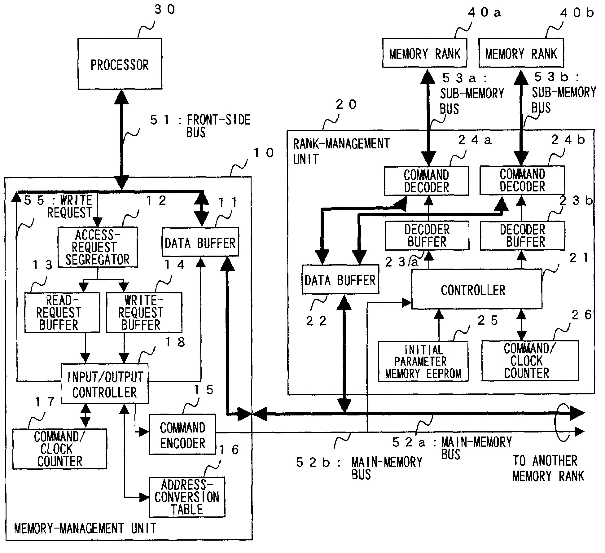
[0043]FIG. 1 is a block drawing showing the construction of the memory-control device of an example of the present invention. In FIG. 1, the memory-control device comprises: a memory-management unit 10 that is connected to a processor 30 via a front-side bus 51; and a rank-management unit 20 that connects to memory ranks 40a, 40b via sub-memory buses 53a, 53b, respectively. The memory-management unit 10 connects to the rank-management unit 20 in memory-module units or rank units via the main memory buses 52a, 52b without directly connecting to the memory ranks 40a, 40b. Here, main memory bus 52a is a bus that transmits data, and main memory bus 52b is a bus that transmits instructions (commands) and addresses. In FIG. 1, an example of a stub connection is shown, however, the connection could also be a tree-type, daisy chain, etc. Also, two memory ranks are shown, however, needless to say, three or more memory ranks could be used. Furthermore, only one memory-manageme...


PUM


Abstract

Improved efficiency of address / data communication over a memory bus. A memory-control device is located between a processor 30 and memory ranks 40a, 40b and controls access to the memory ranks 40a, 40b. A memory-management unit 10 receives and buffers access request from the processor 30 to memory ranks 40a, 40b, and issues access request to a rank-management unit 20 based on scheduling for memory management. A rank-management unit 20 connects the memory ranks 40a, 40b, receives and buffers access request from the memory-management unit 10, and gives access request to a specified memory rank based on scheduling for rank management.

Description

FIELD OF THE INVENTION[0001]This invention relates to a memory-control device, and particularly a technique for accessing a plurality of ranks or memory modules that are connected to the same memory bus.BACKGROUND OF THE INVENTION[0002]When a memory controller receives a memory access request from a processor, and inputs data to or outputs data from a memory such as a DRAM (Dynamic Random Access Memory), the row address and column address are specified, and the memory controller inputs data to or outputs data from the appropriate address. When doing this, it becomes necessary to have a wait time (minimum wait clock necessary for executing an instruction) during each instruction or until the data is actually input or output. This wait time includes a RAS (Row Address Strobe)-to-CAS (Column Address Strobe) delay and CAS latency (CL), and differs depending on the operating speed of the transistor and circuit configuration; also there is a tendency that as the operating frequency become...

Claims


Application Information

Patent Timeline
Patent Type & Authority Patents(United States)
IPC IPC(8): G06F13/14
CPCG06F13/1647
Inventor TAGAWA, FUMITAKE
Owner LONGITUDE SEMICON S A R L
Why Eureka
Try Eureka