Semiconductor structure for low parasitic gate capacitance
a technology of low parasitic gate capacitance and semiconductor structure, which is applied in the direction of semiconductor devices, basic electric elements, electrical appliances, etc., can solve the problems of reducing the performance of transistors, reducing switching speed, and high parasitic capacitance between gate electrodes and contacts
- Summary
- Abstract
- Description
- Claims
- Application Information
AI Technical Summary
Benefits of technology
Problems solved by technology
Method used
Image
Examples
first embodiment
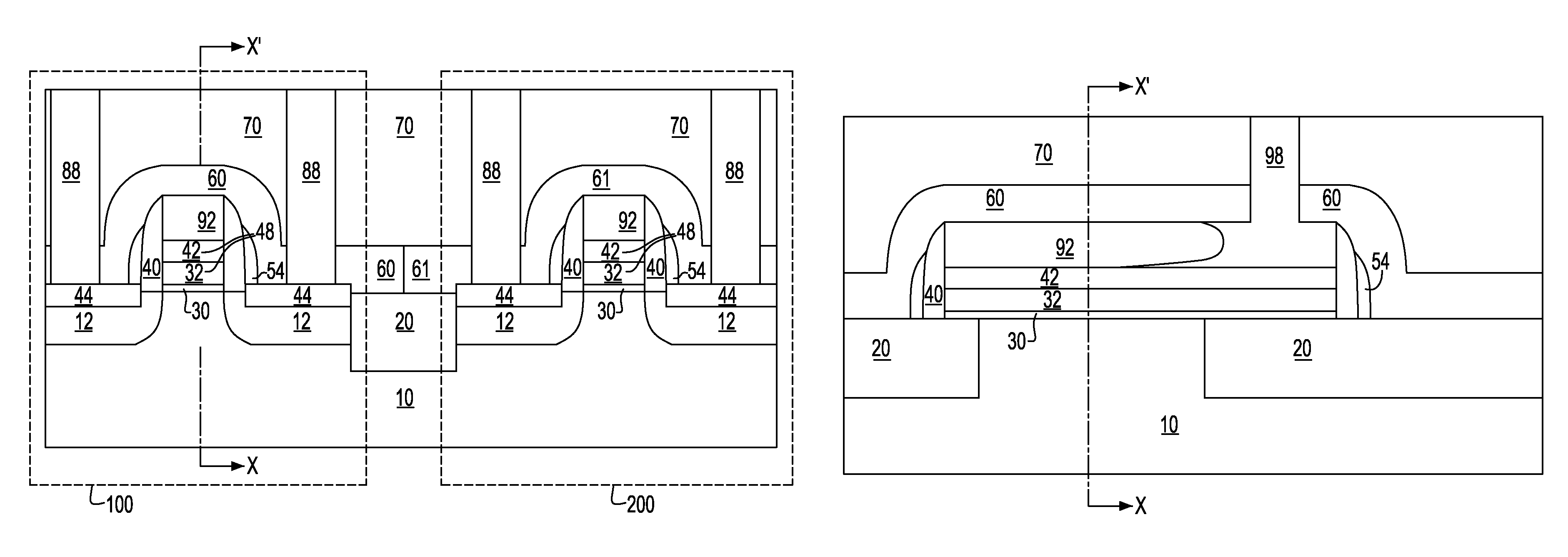
[0069]Referring to FIGS. 11A and 11B, the exemplary semiconductor structure according to the present invention is shown. The contact via holes (80, 90) are filled with metal to form contact vias (88, 98). The contact vias (88, 98) comprise substrate contact vias 88 and gate contact vias 98. The contact vias (88, 98) may be formed, for example, by chemical vapor deposition (CVD) of a metal film with reactant gases containing a metallic precursor gas such as tungsten hexafluoride (WF6). The portion of the metal film deposited above the MOL dielectric 70 may be removed by a blanket etch, chemical mechanical planarization (CMP), or a combination of both.
[0070]According to the first embodiment of the present invention, the low-k dielectric gate filler 52 directly contacts the inner sidewalls of the gate spacer 40 and the top surface of the gate silicide 42. The low-k dielectric gate filler 52 comprises a dielectric material with a dielectric constant of about 3.0 or less. The low-k secon...
fourth embodiment
[0079]According to the present invention, the cavity 92 directly contacts the inner sidewalls of the gate spacer 40 and the top surface of the gate silicide 42. The cavity 92 also contacts a bottom surface of either the first nitride liner 60 or the second nitride liner 61. At least one gate contact via 98 contacts the gate silicide 42 and plugs the corresponding at least one gate contact via hole 90. Therefore, the cavity 92 is enclosed by the inner sidewalls of the gate spacer 40, the top surface of the gate silicide 42, the bottom surface of either the first nitride liner 60 or the second nitride liner 61, and the at least one gate contact via 98. The top of the cavity 92 may be flush with the top of the gate spacer 40 or may be recessed relative to the top of the gate conductor 40.
[0080]The low-k secondary gate spacer 54 may be, or may not be, located directly on the gate spacer 40 and the source and drain silicide 44. The low-k secondary gate spacer 54 comprises a dielectric ma...
PUM
 Abstract
Description
Claims
Application Information


