

Apparatus and method for obtaining topographical dark-field images in a scanning electron microscope
a scanning electron microscope and dark-field image technology, applied in the field of apparatus and methods for electron beam imaging, can solve the problems of incompatibility of the lower-lens configuration with the final (objective) lens, interference with the collection efficiency of the below-the-lens detector, and the polar angle discrimination threshold is not well controlled for such below-the-lens detectors
- Summary
- Abstract
- Description
- Claims
- Application Information
AI Technical Summary
Problems solved by technology
Method used
Image

Examples
Embodiment Construction
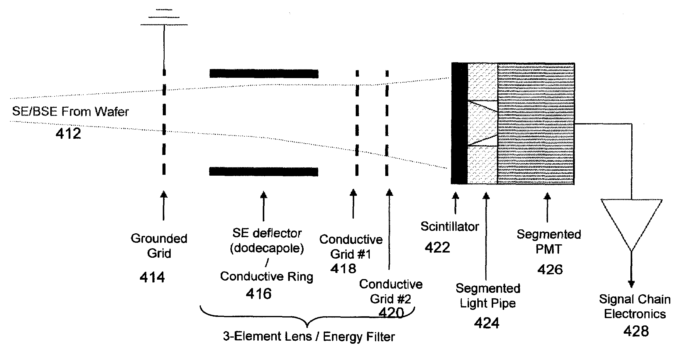
[0023]The present application discloses a behind-the-lens-dark-field (BLDF) configuration which is designed to act as a detector in a scanning electron microscope (SEM). The BLDF configuration has multiple detection elements that are designed to efficiently collect signals for the generation of images giving multiple perspectives of a surface of a sample substrate. The multiple perspectives include so-called dark-field (DF) and bright-field (BF) perspectives.
[0024]DF images typically highlight wafer topography. DF images primarily use the signal from secondary electrons (SE) and / or backscattered electrons (BSE) emitted from the sample with higher polar angles (i.e. with trajectories closer to the surface). BF images (which are more conventional than DF images) typically highlight material contrast and provide higher-resolution, planar images of the sample surface. BF images primarily use SE and / or BSE that are emitted from the sample with lower polar angles (i.e. with trajectories c...
PUM
 Abstract
Description
Claims
Application Information