Electrical antifuse with integrated sensor

an anti-fuse and integrated technology, applied in the direction of emergency protective devices, basic electric elements, heating/cooling contact switches, etc., can solve the problems that anti-fuses in the prior art typically require dielectric breakdown, and achieve the effect of improving the reliability of anti-fuse programming

Active Publication Date: 2010-05-11
TWITTER INC
View PDF41 Cites 45 Cited by
  • Summary
  • Abstract
  • Description
  • Claims
  • Application Information

AI Technical Summary

Benefits of technology

[0008]The cathode and anode have low resistance and conducts electricity. The absence of conducting material in the middle portion of the antifuse link raises the resistance of the antifuse link about 10˜1000 times that of the cathode or anode. The resistance of the antifuse link is tunable by adjusting the doping of the semiconducting material or the dimensions of the middle portion of the antifuse link.

Problems solved by technology

Antifuses in the prior art typically require breakdown of dielectrics by electrical bias and / or heat.

Method used


Image

  • Electrical antifuse with integrated sensor
  • Electrical antifuse with integrated sensor
  • Electrical antifuse with integrated sensor

Examples


first embodiment

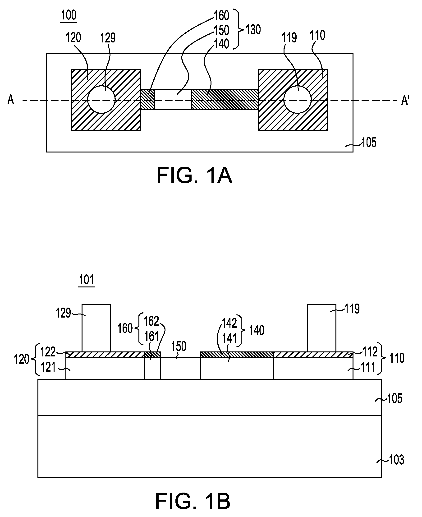
[0033]Referring first to FIGS. 1A and 1B, there is shown an intact antifuse structure 100 according to this invention where an antifuse link 130 is adjoined by a cathode 110 on one side and adjoined by an anode 120 on another side. Preferably, the antifuse link 130, cathode 110, and anode 120 are formed on a shallow trench isolation 105 formed as an insulator on a semiconductor substrate 103. The antifuse link 130 comprises a portion 150 without conducting material and two conducting material containing portions. A first conducting material containing portion 140 of the antifuse link 130 comprises a first volume 141 with a semiconductor material and a second volume 142 with a conducting material. A second conducting material containing portion 160 of the antifuse link 130 comprises a first volume 161 with semiconductor material and a second volume 162 with the conducting material. The first portion 140 of the antifuse link 130 adjoins the cathode 110 and the second portion 160 of th...

second embodiment

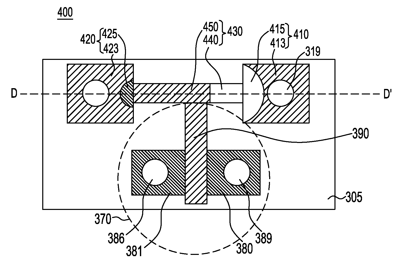
[0045]In FIG. 4A, an intact integrated antifuse 300 with integrated sensing device 370 according to this invention is shown. A cross-sectional view 301 along the line B-B′ in FIG. 4A is shown in FIG. 4B and another cross-sectional view 302 along the line C-C′ in FIG. 4A is shown in FIG. 4C. An antifuse link 330 is adjoined by a cathode 310 on one side and adjoined by an anode 320 on another side. A sensing device 370, that is, a transistor, is placed adjacent to the antifuse link 330 such that the gate 390 of the sensing device 370 is attached to the antifuse link 330. Preferably, the antifuse link 330, cathode 310, and anode 320 are formed on a shallow trench isolation 305 formed as an insulator on a semiconductor substrate 303.

[0046]The antifuse link 330 comprises a portion 350 without conducting material and two conducting material containing portions. A first conducting material containing portion 340 of the antifuse link 330 comprises a first volume 341 with semiconductor mater...

third embodiment

[0057]According to this invention, integrated antifuses 820 are wired in a two-dimensional integrated antifuse array 800 and share programming transistors and sensing circuitry in the periphery. Each of the integrated antifuses 820 has one antifuse structure 840 and one sensing device 860. The cathode 842 of each antifuse structure 840 is connected to one of the column antifuse wiring lines 835 that pass by the same antifuse structure 840. The anode 841 of each antifuse structure 840 is connected to one of the row antifuse wiring lines 845 that pass by the same antifuse structure 840. The drain 861 of each sensing device 860 is connected to one of the sensing device wiring lines 875. The source 862 of each sensing device 860 is connected to one of the column grounding bus 859 and is eventually connected to the ground.

[0058]Programming of the antifuses in the third embodiment of this invention proceeds as follows. All column antifuse wiring lines 835 and all row antifuse wiring lines...


PUM


Abstract

The present invention provides structures for antifuses that utilize electromigration for programming. By providing a portion of antifuse link with high resistance without conducting material and then by inducing electromigration of the conducting material into the antifuse link, the resistance of the antifuse structure is changed. By providing a terminal on the antifuse link, the change in the electrical properties of the antifuse link is detected and sensed. Also disclosed are an integrated antifuse with a built-in sensing device and a two dimensional array of integrated antifuses that can share programming transistors and sensing circuitry.

Description

FIELD OF THE INVENTION[0001]The present invention relates to a semiconductor memory device, and particularly, to semiconductor antifuse structures.BACKGROUND OF THE INVENTION[0002]Many types of semiconductor fuses and antifuses are known in the art. Both the fuses and antifuses utilize the change in resistance of the individual structure under certain bias conditions. Once programmed, the programmed state of the fuses or antifuses does not revert to the original state on its own; that is, the programmed state of the fuse or the antifuse is not reversible. Thus, fuses and antifuses are conducive to the manufacture of a programmable read only memory (PROM). Programming or lack of programming constitutes one bit of stored information in fuses or antifuses. The difference between fuses and antifuses is the way the resistance of the memory element is changed during the programming process. Semiconductor fuses have a low initial resistance state that may be changed to a higher resistance ...

Claims


Application Information

Patent Timeline
Patent Type & Authority Patents(United States)
IPC IPC(8): H01L29/04H01H37/76
CPCH01L23/5252H01L27/101H01L27/112H01L2924/3011H01L2924/0002H01L2924/00H10B20/00
Inventor KIM, DEOK-KEEKIM, HOKIKOTHANDARAMAN, CHANDRASEKHARANPARK, BYEONGJUSAFRAN, JOHN M.
Owner TWITTER INC
Why Eureka
Try Eureka