System and methods of measuring semiconductor sheet resistivity and junction leakage current

a technology of resistivity and junction leakage current, applied in the direction of resistance/reactance/impedence, instruments, measurement devices, etc., can solve the problems of affecting the operation of active elements, affecting the accuracy of junction leakage current measurement, and limiting the measurement accuracy of sheet resistance as well as the available measurement range. achieve the effect of high test accuracy

Inactive Publication Date: 2010-05-11
FOUR DIMENSIONS
View PDF4 Cites 14 Cited by
  • Summary
  • Abstract
  • Description
  • Claims
  • Application Information

AI Technical Summary

Benefits of technology

[0013]An advantage of the present invention is that the present junction leakage measurement system enables test parameters to be explicitly set and the direct measurement of meaningful current and voltage levels. These parameters include the junction bias potential, which can be both explicitly set and, further, precisely varied for evaluating different operating regimes. The available bias potential range includes the full range of reverse junction bias potentials likely be encountered in expected integrated circuit operation. Direct measurement of operating potentials and currents also enables realization of a high degree of test accuracy, particularly with regard to the sheet resistivity, junction leakage current and conductivity.
[0014]Another advantage of the present invention is that the test system and methods can be utilized to measure a variety of performance related parameters. In addition to sheet resistivity and junction leakage, the system and methods can directly measure the contact resistivity of a superficial metal film, such as a metal silicide conductor, to the underlying semiconductor layer, and contact resistance of an applied electrode to an underlying ion-implanted layer.

Problems solved by technology

Otherwise, operation of the active elements will become dominated by known short channel and other undesirable effects.
Consequently, measurement accuracy as well as the available measurement range of sheet resistance will be limited.
The absence of any bias control makes measurement accuracy of junction leakage currents even less accurate.
Even then, the photo-induced forward bias precludes any meaningful measurement of the junction leakage contribution due to tunning under reverse bias, as will be encountered in normal operating conditions.

Method used


Image

  • System and methods of measuring semiconductor sheet resistivity and junction leakage current
  • System and methods of measuring semiconductor sheet resistivity and junction leakage current
  • System and methods of measuring semiconductor sheet resistivity and junction leakage current

Examples


Embodiment Construction

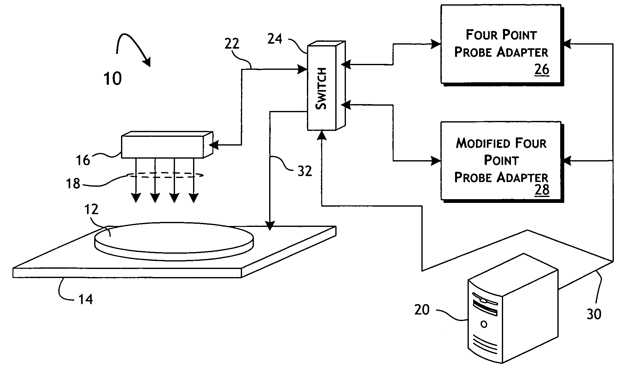
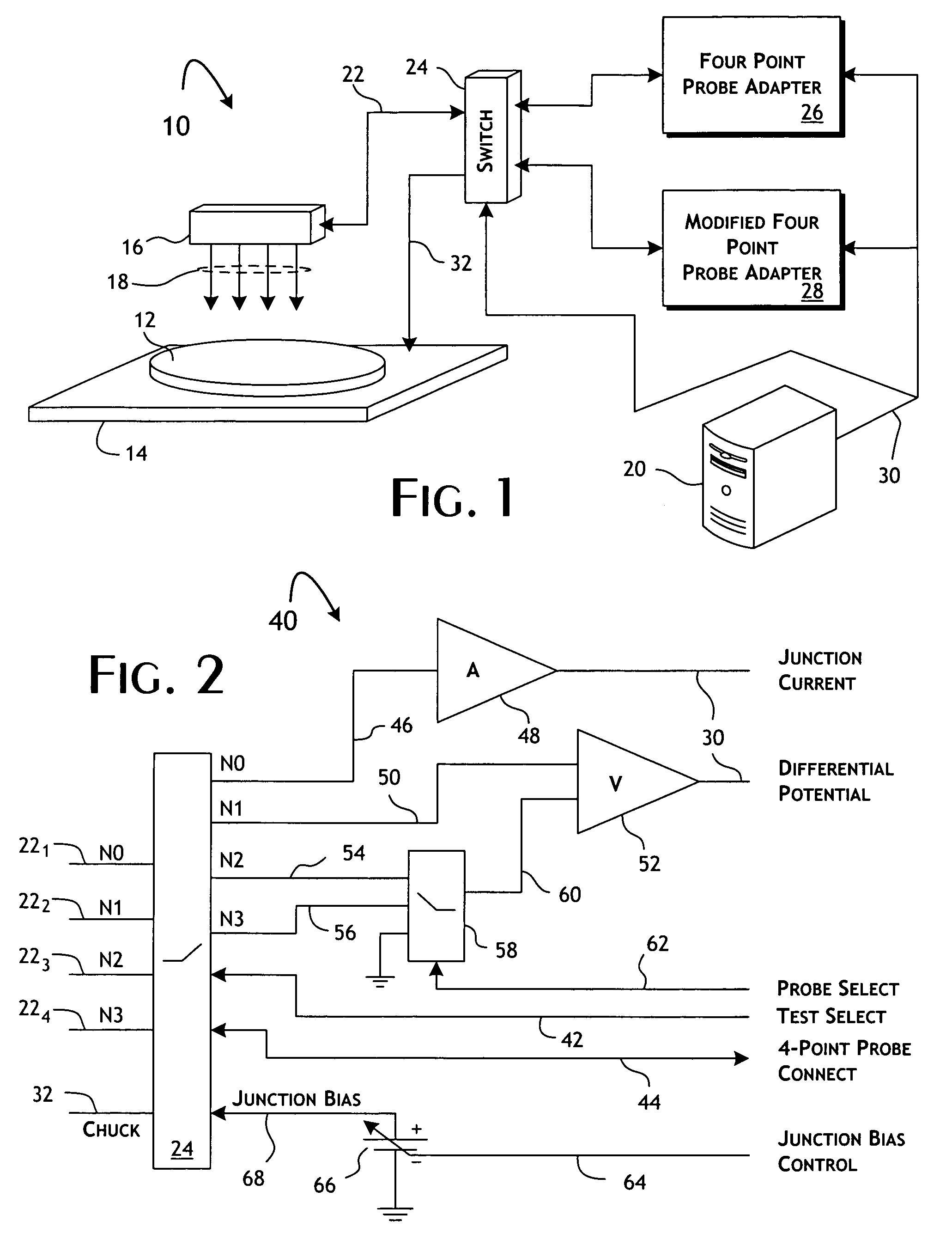
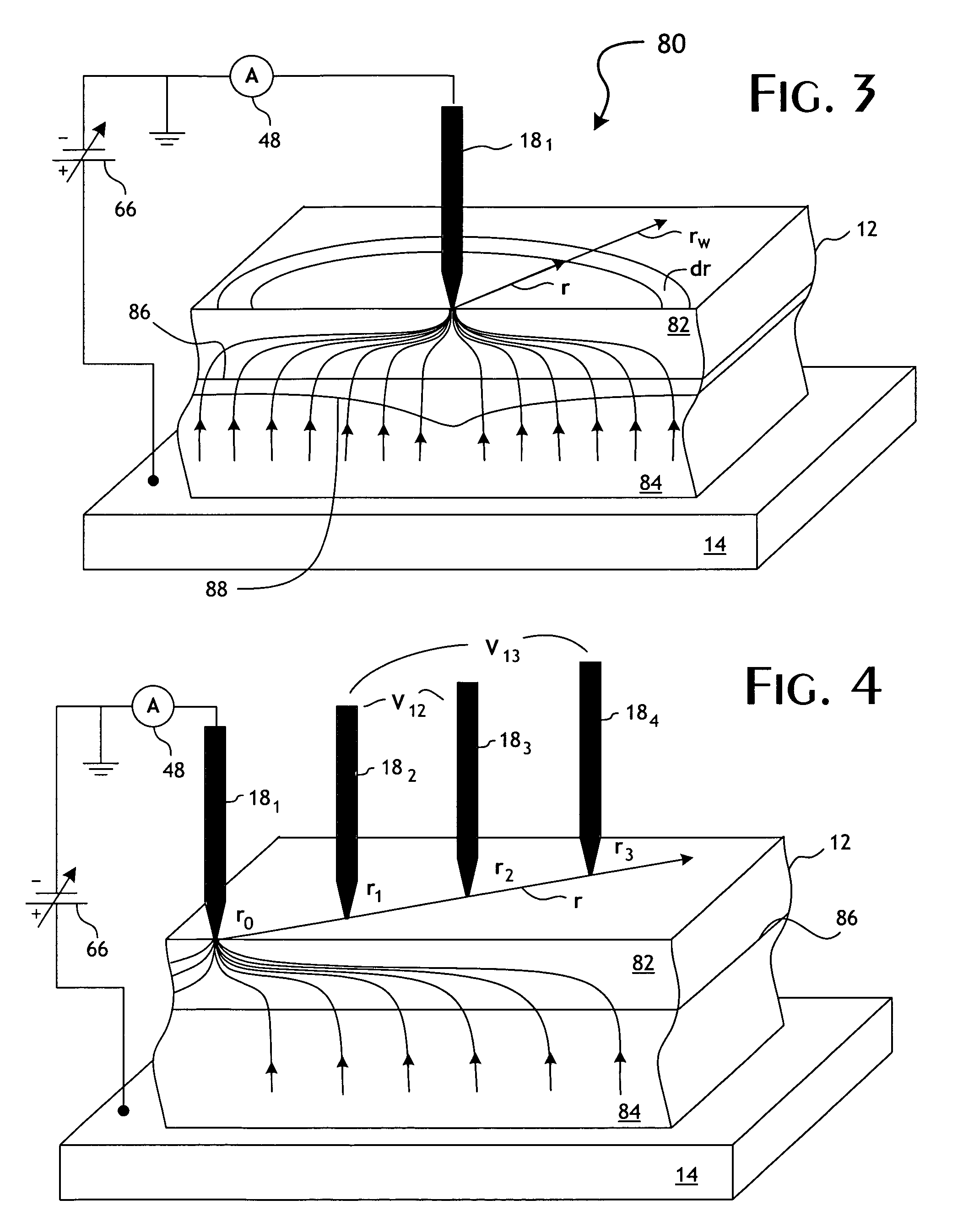
[0019]The present invention provides for the direct measurement of a variety of semiconductor junction related properties important in the in-process production characterization of semiconductor layers. At present, the principal value of the present invention is perceived to be the accuracy and ease of measurement of sheet resistivity and junction leakage current associated with ultra shallow junction (USJ) ion implanted surface layers. While the following discussion will be principally directed to this application, further uses and benefits of the present invention are fully contemplated. In particular, contact resistivity of surface films, including metal and metal silicide films, can be measured by the present invention. In the following detailed description of the invention like reference numerals are used to designate like parts depicted in one ore more of the figures.

[0020]Referring to FIG. 1, a four-point probe test measurement system 10, incorporating modifications in accord...


PUM


Abstract

Sheet resistance, junction leakage and contact conductivity of a semiconductor layer, associated with an ultra-shallow junction layer or metal film are measured by contacting the surface with a plurality of probes. The probes can be used, in conjunction with a four-point probe system, to determine sheet resistivity. Junction leakage through an ultra-shallow junction is determined by establishing a reverse bias across the junction set at a predetermined voltage value, measuring through a first probe a total junction current conduction value, measuring through second, third, and fourth probes a plurality of voltage values. The junction leakage value is then directly computed based on the sheet resistivity value, reverse bias potential, wafer radius, and the measured voltage values. Contact conductivity between a metal film and semiconductor layer can be similarly directly computed.

Description

[0001]This application claims the benefit of U.S. Provisional Application No. 60 / 875,060, filed Dec. 15, 2006.BACKGROUND OF THE INVENTION[0002]1. Field of the Invention[0003]The present invention is generally related to semiconductor manufacturing test measurement systems and, in particular, to the measurement of sheet resistance and junction leakage associated with p-n junctions and conductivity associated with metal films.[0004]2. Description of the Related Art[0005]The active elements of semiconductor devices within an integrated circuit (IC) are constructed in a succession of semiconductor layers, variously created using deposition and ion implantation process steps, and metal film depositions. These layers, particularly including implanted layers, are sensitive to fabrication-dependent process variables. In order to obtain appropriate electrical performance and process yield, implant fabricated layers must be highly uniform, both physically and electrically. Historically, impla...

Claims


Application Information

Patent Timeline
Patent Type & Authority Patents(United States)
IPC IPC(8): G01R31/02
CPCG01R31/2648G01R31/2831
Inventor CHEN, JAMES T. C.DIMITROV, DIMITAR B.
Owner FOUR DIMENSIONS
Why Eureka
Try Eureka