Exponentially doped layers in inverted metamorphic multijunction solar cells

a solar cell and metamorphic technology, applied in the field of solar cell semiconductor devices, can solve the problems of presenting a number of practical difficulties relating to the appropriate choice of materials and fabrication steps, and the inability of solar cells to meet the needs of more sophisticated applications

Active Publication Date: 2010-06-01
SOLAERO TECH CORP
View PDF39 Cites 102 Cited by
  • Summary
  • Abstract
  • Description
  • Claims
  • Application Information

AI Technical Summary

Benefits of technology

[0080]The efficacy of an embodiment of the present invention has been demonstrated in a test solar cell which incorporated an exponential doping profile in the 3 μm thick base layer of the bottom subcell, according to one embodiment of the present invention. Following measurements of the electrical parameters of the test cell, there was observed a 6.7% increase in current collection. The measurements indicated an open circuit voltage (Voc) equal to at least 3.014V, a short circuit current (Jsc) of at least 16.55 mA / cm2, and a fill factor (FF) of at least 0.86 at AMO.

Problems solved by technology

While significant progress has been made in this area, the requirement for solar cells to meet the needs of more sophisticated applications has not kept pace with demand.
The structures described in such prior art present a number of practical difficulties relating to the appropriate choice of materials and fabrication steps.

Method used


Image

  • Exponentially doped layers in inverted metamorphic multijunction solar cells
  • Exponentially doped layers in inverted metamorphic multijunction solar cells
  • Exponentially doped layers in inverted metamorphic multijunction solar cells

Examples


Embodiment Construction

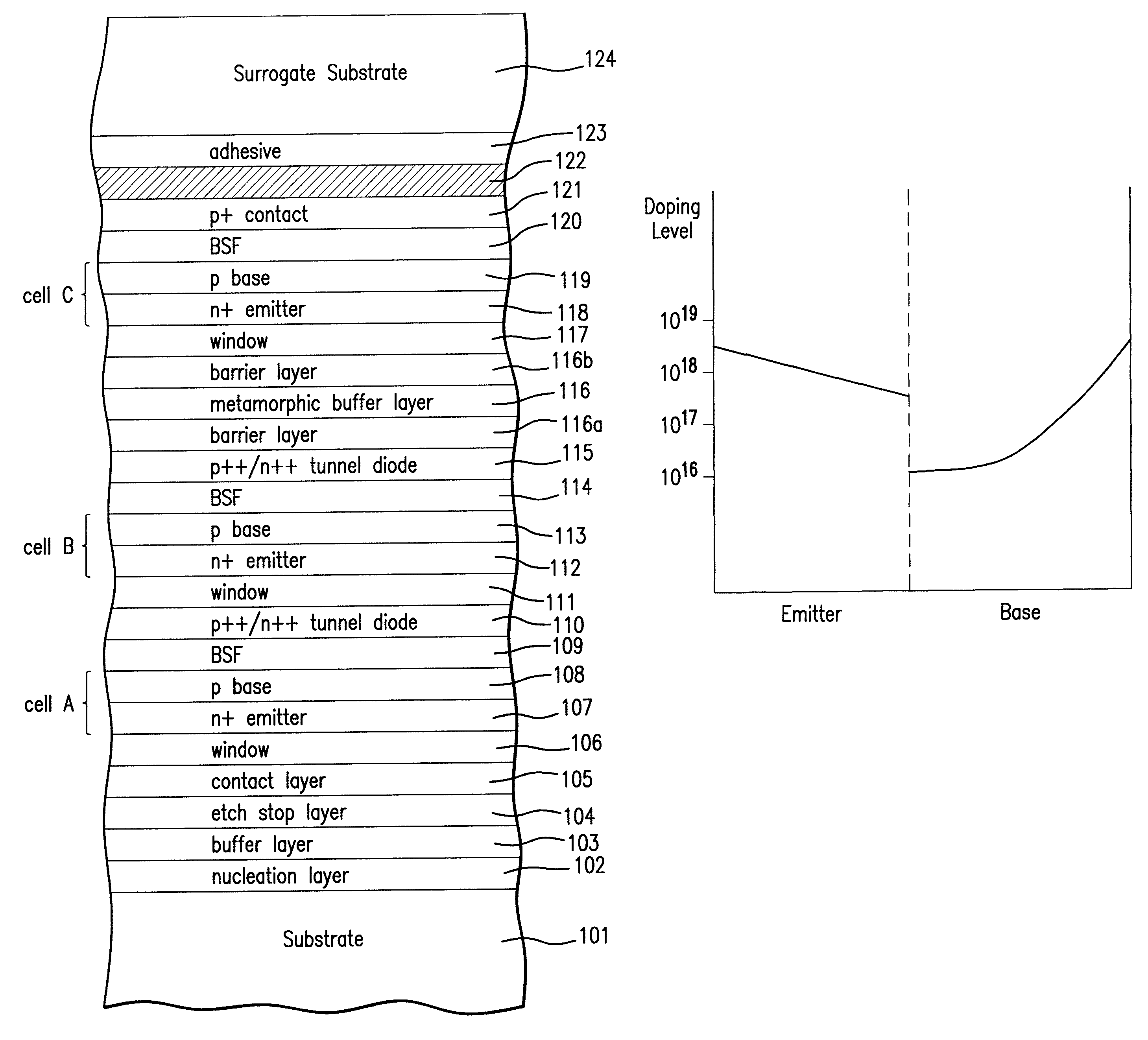
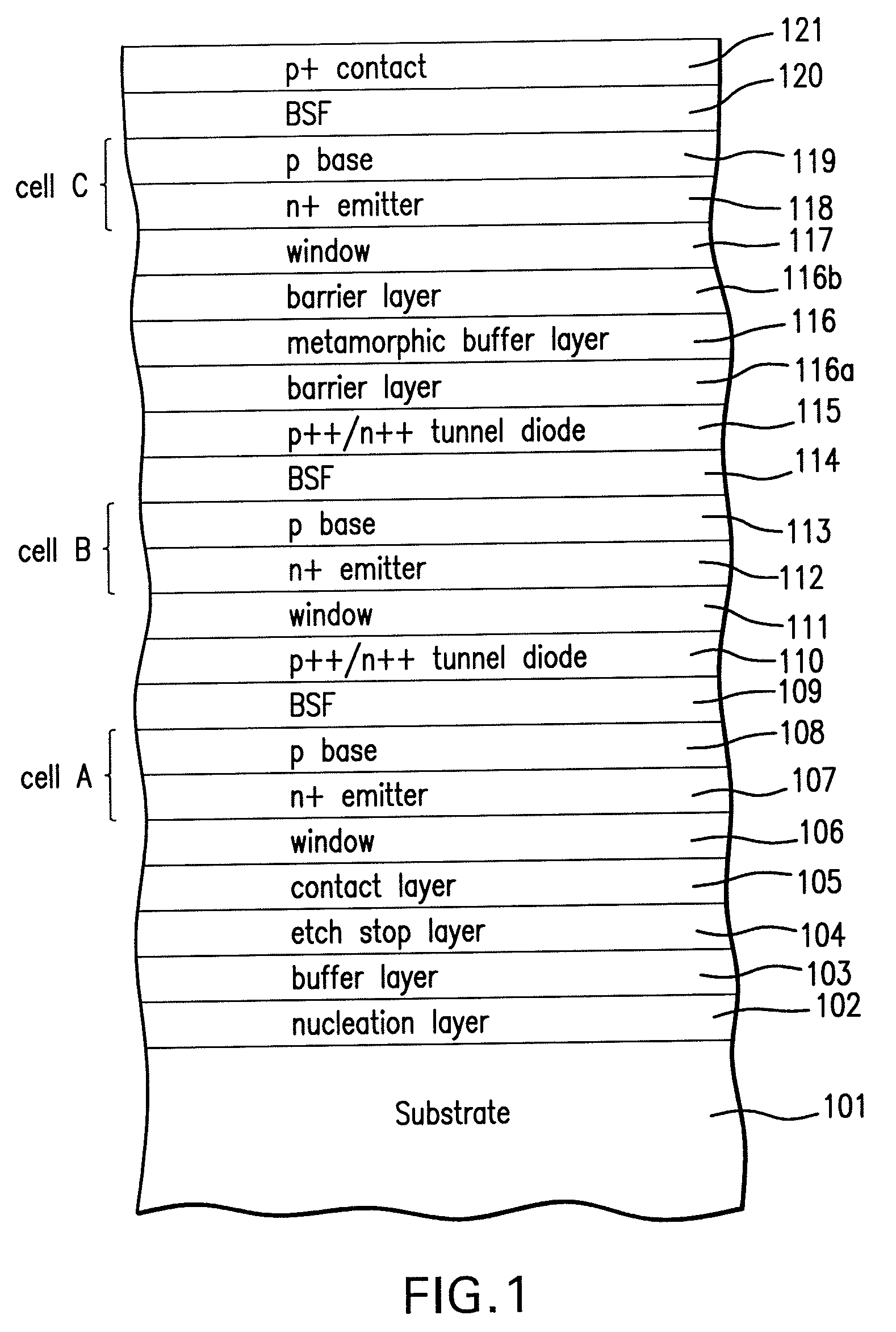
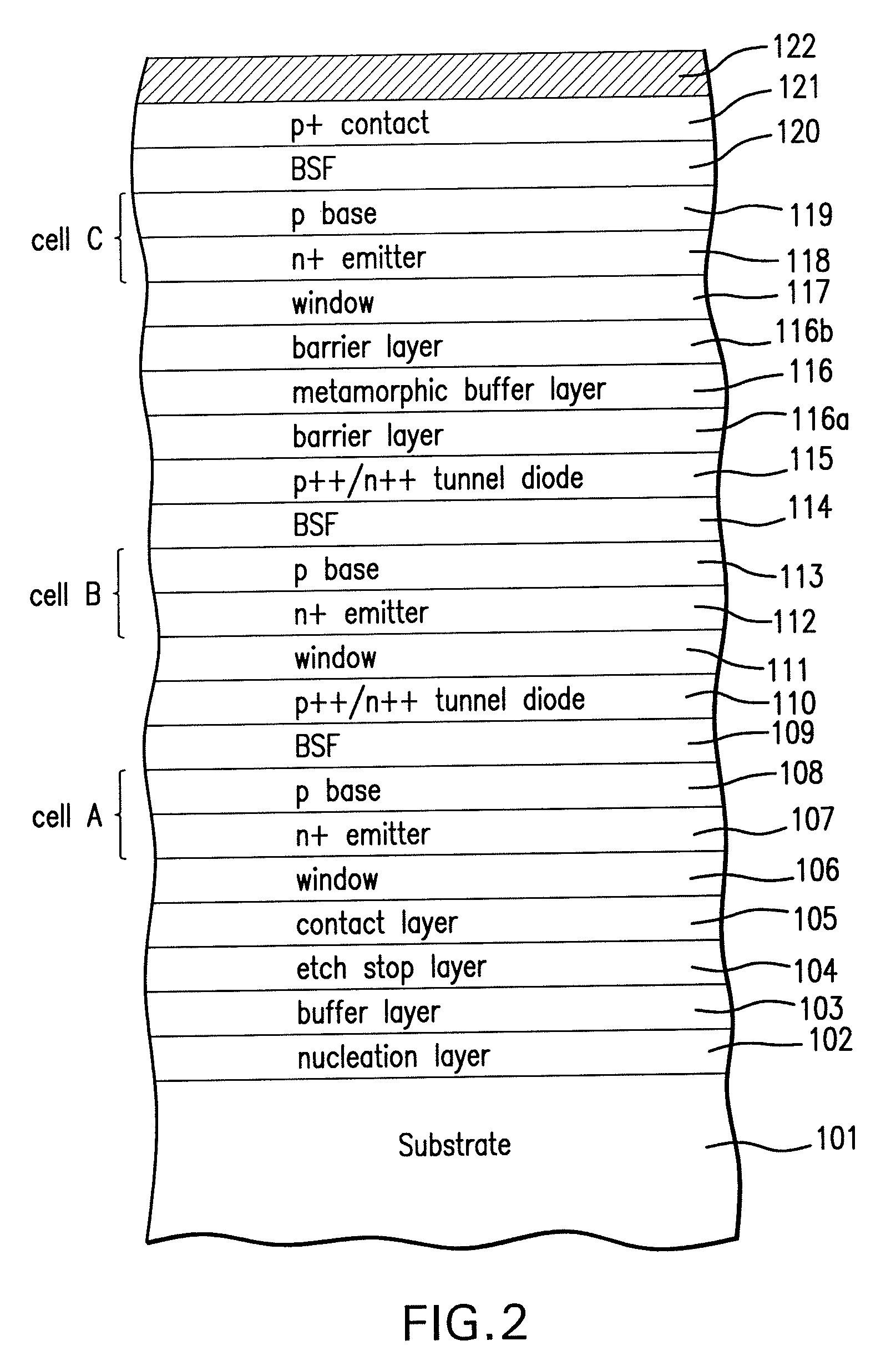
[0038]Details of the present invention will now be described including exemplary aspects and embodiments thereof. Referring to the drawings and the following description, like reference numbers are used to identify like or functionally similar elements, and are intended to illustrate major features of exemplary embodiments in a highly simplified diagrammatic manner. Moreover, the drawings are not intended to depict every feature of the actual embodiment nor the relative dimensions of the depicted elements, and are not drawn to scale.

[0039]Reference throughout this specification to “one embodiment” or “an embodiment” means that a particular feature, structure, or characteristic described in connection with the embodiment is included in at least one embodiment of the present invention. Thus, the appearances of the phrases “in one embodiment” or “in an embodiment” in various places throughout this specification are not necessarily all referring to the same embodiment. Furthermore, the ...


PUM

PropertyMeasurementUnit
thicknessaaaaaaaaaa
thicknessaaaaaaaaaa
thicknessaaaaaaaaaa

Abstract

A method of forming a multijunction solar cell including an upper subcell, a middle subcell, and a lower subcell, including providing first substrate for the epitaxial growth of semiconductor material; forming a first solar subcell on the substrate having a first band gap; forming a second solar subcell over the first solar subcell having a second band gap smaller than the first band gap; forming a grading interlayer over the second subcell, the grading interlayer having a third band gap greater than the second band gap; and forming a third solar subcell over the grading interlayer having a fourth band gap smaller than the second band gap such that the third subcell is lattice mis-matched with respect to the second subcell, wherein at least one of the bases of a solar subcell has an exponentially doped profile.

Description

REFERENCE TO RELATED APPLICATIONS[0001]This application is a divisional patent application of U.S. patent application Ser. No. 11 / 956,069, filed on Dec. 13, 2007 (pending).[0002]This application is related to co-pending U.S. patent application Ser. Nos. 11 / 860,142 and 11 / 860,183 filed Sep. 24, 2007.[0003]This application is related to co-pending U.S. patent application Ser. No. 11 / 836,402 filed Aug. 8, 2007.[0004]This application is also related to co-pending U.S. patent application Ser. No. 11 / 616,596 filed Dec. 27, 2006.[0005]This application is also related to co-pending U.S. patent application Ser. No. 11 / 445,793 filed Jun. 2, 2006.GOVERNMENT RIGHTS STATEMENT[0006]This invention was made with government support under Contract No. FA9453-06-C-0345 awarded by the U.S. Air Force. The Government has certain rights in the invention.BACKGROUND OF THE INVENTION[0007]1. Field of the Invention[0008]The present invention relates to the field of solar cell semiconductor devices, and partic...

Claims


Application Information

Patent Timeline
Patent Type & Authority Patents(United States)
IPC IPC(8): H01L21/00
CPCH01L31/03042H01L31/03046H01L31/0693H01L31/1844H01L31/06875Y02E10/544Y02P70/50
Inventor STAN, MARK A.CORNFELD, ARTHURLEY, VANCE
Owner SOLAERO TECH CORP
Why Eureka
Try Eureka