Stress-distribution detecting semiconductor package group and detection method of stress distribution in semiconductor package using the same

a semiconductor and stress distribution technology, applied in the direction of mechanical measurement arrangement, mechanical instruments, using mechanical means, etc., can solve the problems of affecting the production of ics with highly accurate electrical properties, property change, compressive stress over the surface of the semiconductor chip,

Inactive Publication Date: 2010-06-15
RICOH ELECTRONIC DEVICES CO LTD
View PDF6 Cites 12 Cited by
  • Summary
  • Abstract
  • Description
  • Claims
  • Application Information

AI Technical Summary

Problems solved by technology

The demand has increased not only for size reduction but also for high accuracy, and increasing the initial accuracy of analog ICs and minimizing the property variations, for example, are major technical challenges for device development.
One factor that impedes producing ICs having highly accurate electrical properties is property change in a semiconductor device associated with a molded package process.
A property change occurs as a molding resin having a high linear expansion coefficient hardens and contracts in a resin encapsulation process, which causes compressive stress over the surface of the semiconductor chip.
For various devices, the piezoelectric effect due to this compressive stress causes change in their electrical properties, which then results in changing their circuit characteristics having been obtained at wafer level.
However, if an equal number of electrode pads are provided for the finished semiconductor chip and for the stress-distribution detecting semiconductor chip, the number of piezoelectric resistive elements on the stress-distribution detecting semiconductor chip is limited by the number of electrode pads of the finished semiconductor chip, and accordingly a conventional stress-distribution detecting semiconductor chip is not able to thoroughly detect the stress distribution over the entire extent of the semiconductor chip.
That is to say, change in the resistance of the piezoelectric resistive elements can be measured at only two to four positions on the stress-distribution detecting semiconductor chip, thus leaving a problem of not being able to thoroughly detect the stress distribution over the entire extent of the semiconductor chip.

Method used


Image

  • Stress-distribution detecting semiconductor package group and detection method of stress distribution in semiconductor package using the same
  • Stress-distribution detecting semiconductor package group and detection method of stress distribution in semiconductor package using the same
  • Stress-distribution detecting semiconductor package group and detection method of stress distribution in semiconductor package using the same

Examples


Embodiment Construction

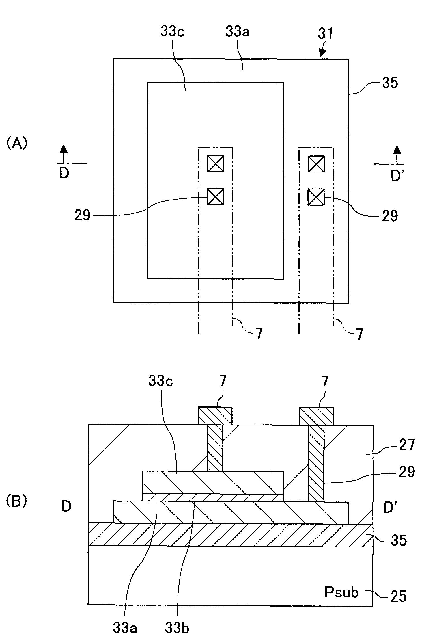
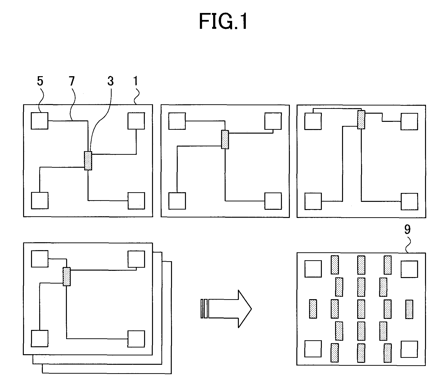
[0028]FIG. 1 illustrates one embodiment of a stress-distribution detecting semiconductor package group of the present invention, and shows a schematic plan view of an arrangement of electrode pads and a piezoelectric resistive element on a stress detecting semiconductor chip of each stress-distribution detecting semiconductor package. In this embodiment, piezoelectric resistive elements formed of diffusion resistances are used as piezoelectric elements for stress detection.

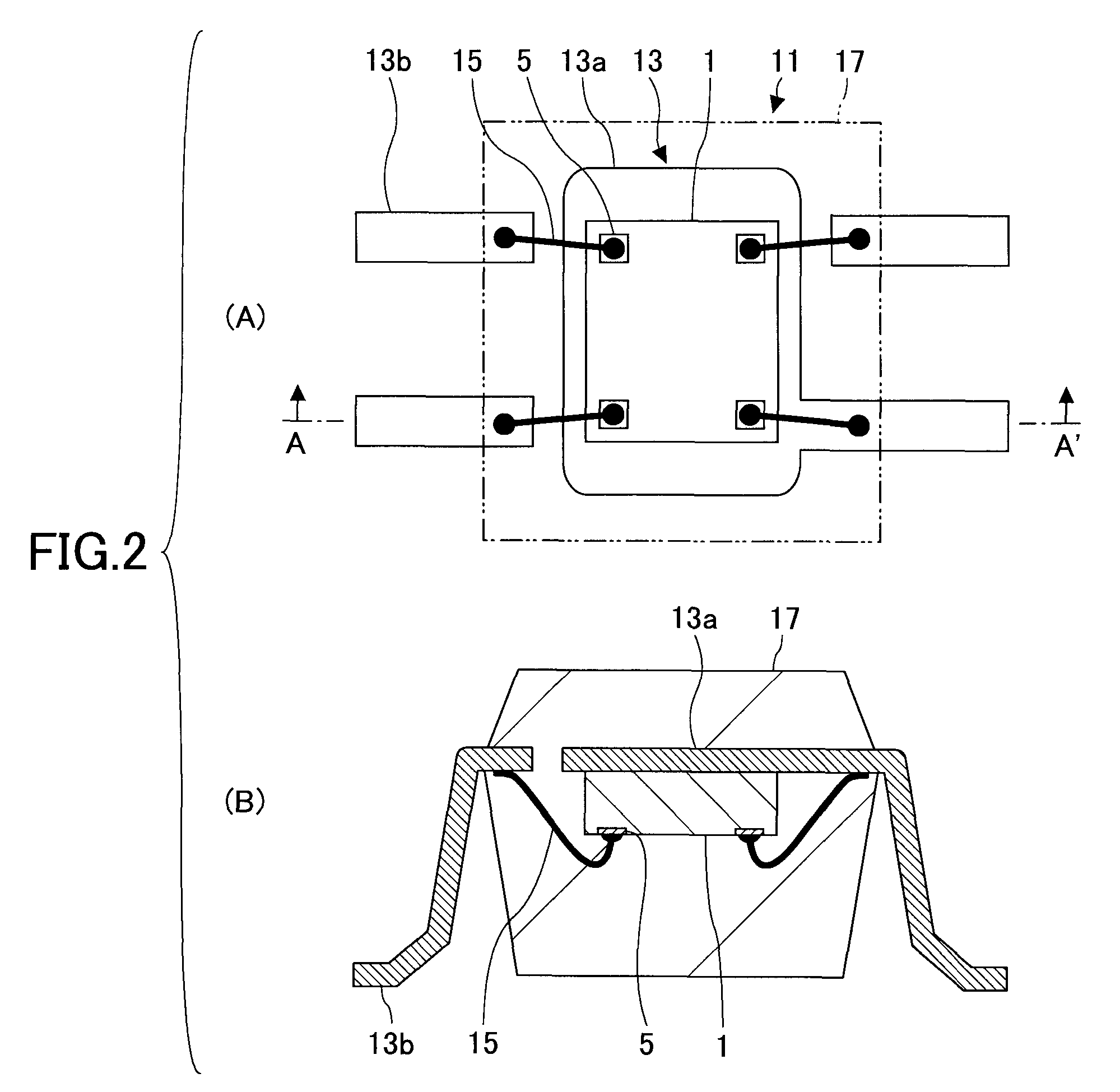
[0029]The stress-distribution detecting semiconductor package group of the present embodiment comprises, for instance, seventeen stress-distribution detecting semiconductor packages. In each stress-distribution detecting semiconductor package, a stress detecting semiconductor chip 1 includes one piezoelectric resistive element 3 and four electrode pads 5. The plane size of each stress detecting semiconductor chip 1 is 0.8 mm by 0.7 mm, for example. The plane size of the piezoelectric resistive element 3 is 2 μm by...


PUM


Abstract

A disclosed stress-distribution detecting semiconductor package group includes multiple stress-distribution detecting semiconductor packages each formed by resin-encapsulating a stress detecting semiconductor chip of the same size using an identical resin encapsulation structure. Each stress detecting semiconductor chip includes a piezoelectric element for stress detection and at least two electrode pads electrically connected to the piezoelectric element to measure an electrical property of the piezoelectric element. The piezoelectric elements of the stress detecting semiconductor chips are respectively disposed on the corresponding stress detecting semiconductor chips to be located at different positions from one another when superimposed on a single imaginary semiconductor chip plane having the same plane size as that of the stress detecting semiconductor chips.

Description

BACKGROUND OF THE INVENTION[0001]1. Field of the Invention[0002]The present invention relates to a stress-distribution detecting semiconductor package group used to detect stress distribution in a resin-encapsulated semiconductor package, and also relates to a detection method of stress distribution in a semiconductor package (hereinafter, referred to as “semiconductor-package stress-distribution detection method”) using the stress-distribution detecting semiconductor package group.[0003]2. Description of the Related Art[0004]With the recent rapid growth in popularity of portable electronic devices, there is a demand for reducing the size of electronics used in such portable electronic devices, and ICs (Integrated Circuits) are no exception. The demand has increased not only for size reduction but also for high accuracy, and increasing the initial accuracy of analog ICs and minimizing the property variations, for example, are major technical challenges for device development.[0005]O...

Claims


Application Information

Patent Timeline
Patent Type & Authority Patents(United States)
IPC IPC(8): G01B7/16
CPCG01L1/2293G01L1/16H01L2224/05554H01L2224/16225H01L2224/48091H01L2224/48247H01L2224/48257H01L2224/48465H01L2924/1305H01L2924/13091H01L2924/15311H01L2924/00014H01L2924/00
Inventor UEDA, NAOHIROWATANABE, HIROFUMI
Owner RICOH ELECTRONIC DEVICES CO LTD
Why Eureka
Try Eureka