Floating body memory and method of fabricating the same

a floating body memory and memory technology, applied in the field of semiconductor devices, can solve the problems of reducing the operating speed of the transistor, presenting a number of difficulties in high-integration dram cells,

Inactive Publication Date: 2010-06-22
SAMSUNG ELECTRONICS CO LTD
View PDF49 Cites 172 Cited by
  • Summary
  • Abstract
  • Description
  • Claims
  • Application Information

AI Technical Summary

Problems solved by technology

However, highly integrating the DRAM cells presents a number of difficulties.
When the source and drain regions of the transistor have large junction areas, a junction capacitance of the source and drain regions increases, which leads to a decrease in the operating speed of the transistor.

Method used


Image

  • Floating body memory and method of fabricating the same
  • Floating body memory and method of fabricating the same
  • Floating body memory and method of fabricating the same

Examples


Embodiment Construction

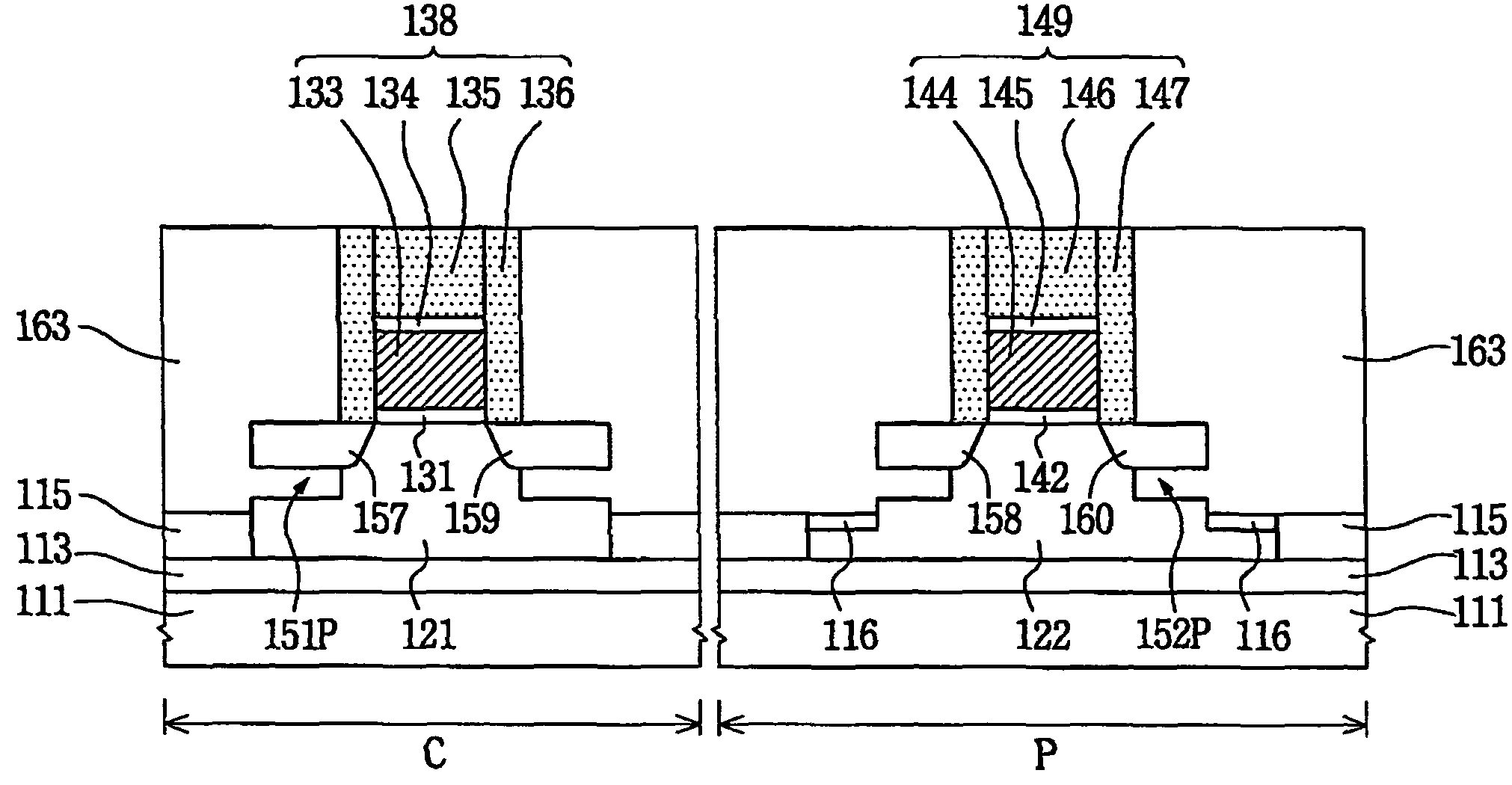
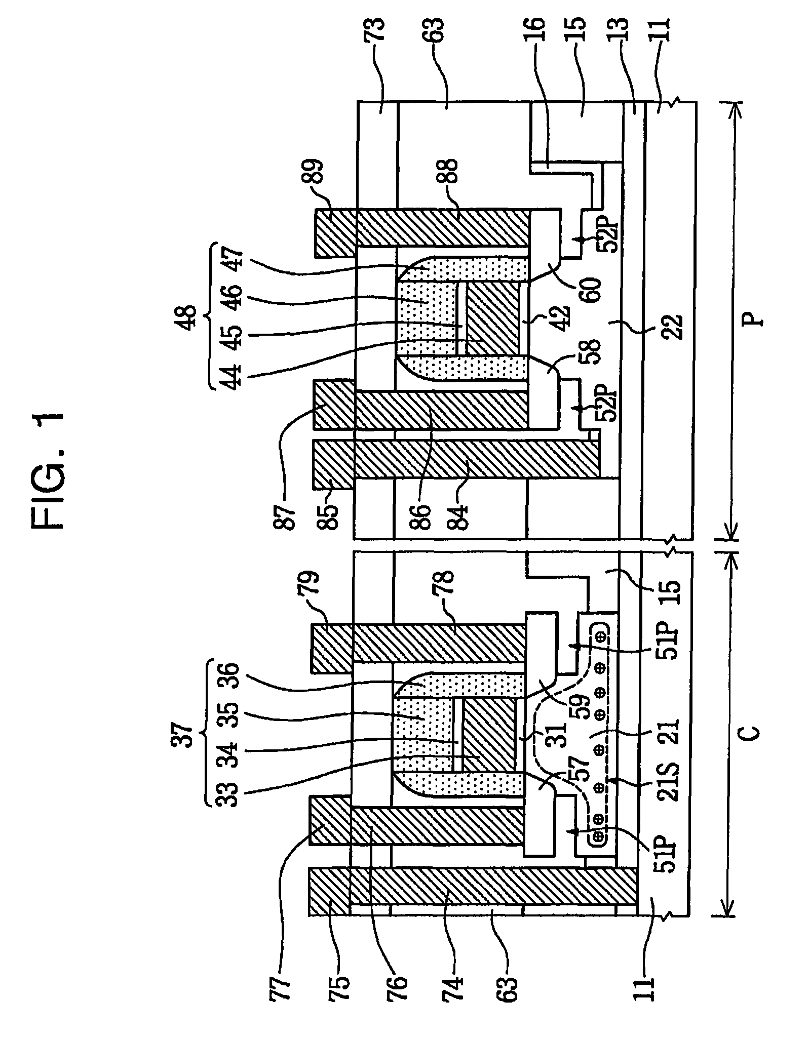
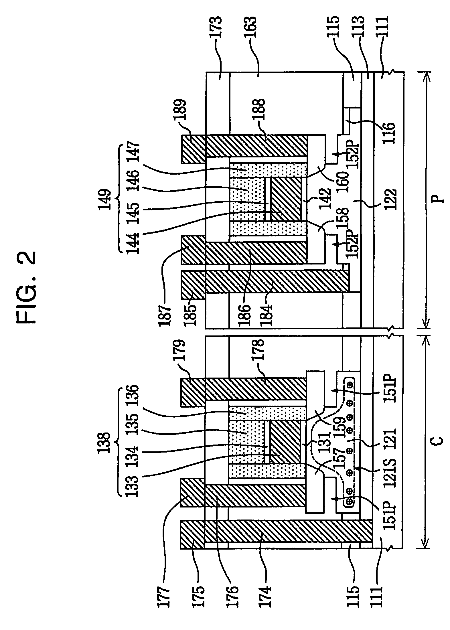
[0029]The present invention will now be described more fully with reference to the accompanying drawings, in which exemplary embodiments of the invention are shown. The invention, however, may be embodied in various different forms, and should not be construed as being limited only to the illustrated embodiments. Rather, these embodiments are provided as examples, to convey the concept of the invention to one skilled in the art. Accordingly, known processes, elements, and techniques are not described with respect to some of the embodiments of the present invention. In the drawings, the thicknesses of layers and regions are exaggerated for clarity. In addition, when a layer is described to be formed on another layer or on a substrate, it is intended to mean that the layer may be formed directly on the other layer or on the substrate, or another layer may be interposed between the layer and the other layer and / or substrate. Throughout the drawings and written description, like referen...


PUM


Abstract

A floating body memory includes a semiconductor substrate having a cell region and a peripheral circuit region. A floating body cell is located in the cell region and a first floating body is located in the peripheral circuit region of the semiconductor substrate. A peripheral gate pattern is positioned on the first floating body. First source and drain regions are positioned at both sides of the peripheral gate pattern. First leakage shielding patterns are positioned between the first floating body and the first source and drain regions, the first source and drain regions contacting the first floating body. The first leakage shielding patterns may be positioned outside outer edges of the peripheral gate pattern.

Description

CROSS-REFERENCE TO RELATED APPLICATION[0001]A claim of priority is made to Korean Patent Application No. 10-2006-0126831, filed Dec. 13, 2006, the subject matter of which is hereby incorporated by reference.BACKGROUND OF THE INVENTION[0002]1. Field of the Invention[0003]The present invention relates to a semiconductor device and a method of fabricating the same, and more particularly, to a floating body memory having leakage shield patterns and a method of fabricating the same.[0004]2. Description of the Related Art[0005]In general, a semiconductor memory includes a cell region and a peripheral circuit region. Memory cells are located in the cell region, and driving devices necessary to operate the memory cells, such as transistors, are located in the peripheral circuit region.[0006]Dynamic random access memory (DRAM) cells, which is a type nonvolatile memory device, are widely used as the memory cells. Typically, DRAM cells include one capacitor, one transistor and interconnections...

Claims


Application Information

Patent Timeline
Patent Type & Authority Patents(United States)
IPC IPC(8): H01L29/788
CPCH01L21/84H01L27/108H01L29/7841H01L27/10844H01L27/1203H01L27/10802H10B12/20H10B12/00H10B12/01H10B99/00
Inventor TAK, NAM-KYUNSONG, KI-WHAN
Owner SAMSUNG ELECTRONICS CO LTD
Why Eureka
Try Eureka