Polarizing optical device, liquid crystal display using the same and method of making the same
a technology of optical devices and liquid crystal displays, applied in the direction of optics, instruments, optical elements, etc., can solve the problems of difficult to manufacture combinations, and difficult to meet the requirements of a large number of materials, etc., to achieve high optical efficiency, high contrast display, and easy manufacturing
- Summary
- Abstract
- Description
- Claims
- Application Information
AI Technical Summary
Benefits of technology
Problems solved by technology
Method used
Image
Examples
first embodiment
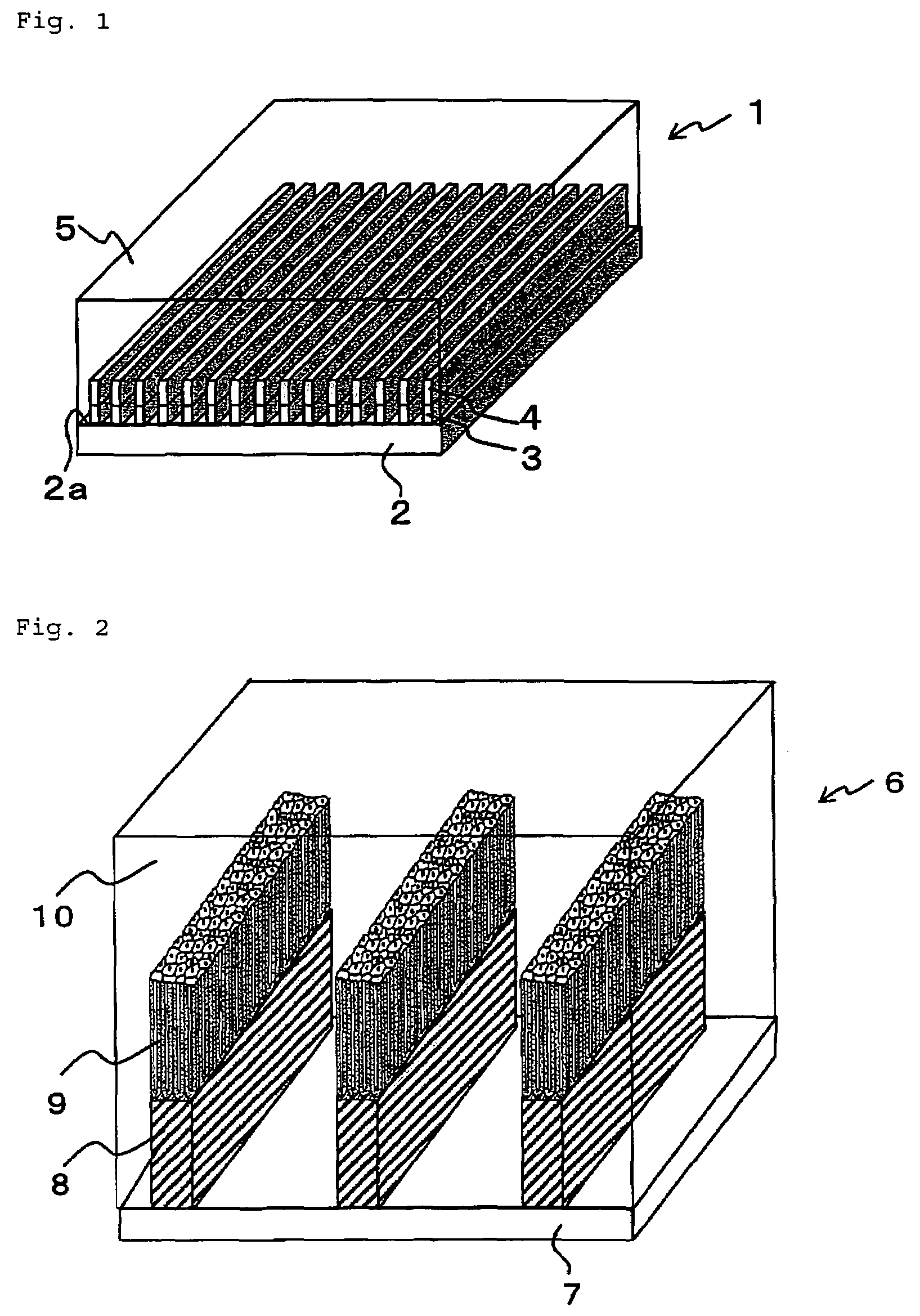
[0038]FIG. 1 illustrates a polarizing optical device 1 according to a first embodiment of the present invention. The polarizing optical device 1 may include a substrate 2. The substrate 2 may include an extrafine metal grid structure 3 on one major surface 2a thereof with A compound metal part 4 may be formed by surface treating an upper surface of the extrafine metal grid structure 3.
[0039]The substrate 2 may be made of, for example, optically transparent glass or resin film, e.g., polyethylene terephthalate (PET), polycarbonate (PC), polymethyl methacrylate (PMMA), etc. The extrafine metal grid structure 3 may be made of, e.g., wires having a high optical reflectance, and may have a height of about 300 nm. A wire width, a wire distance, and an average grid pitch of the extrafine metal grid structure 3 may be set to be, e.g., about 50 nm, about 100 nm, and about 150 nm, respectively.
[0040]The compound metal part 4 may be formed on outer layers of the wires. Specifically, the compou...
second embodiment
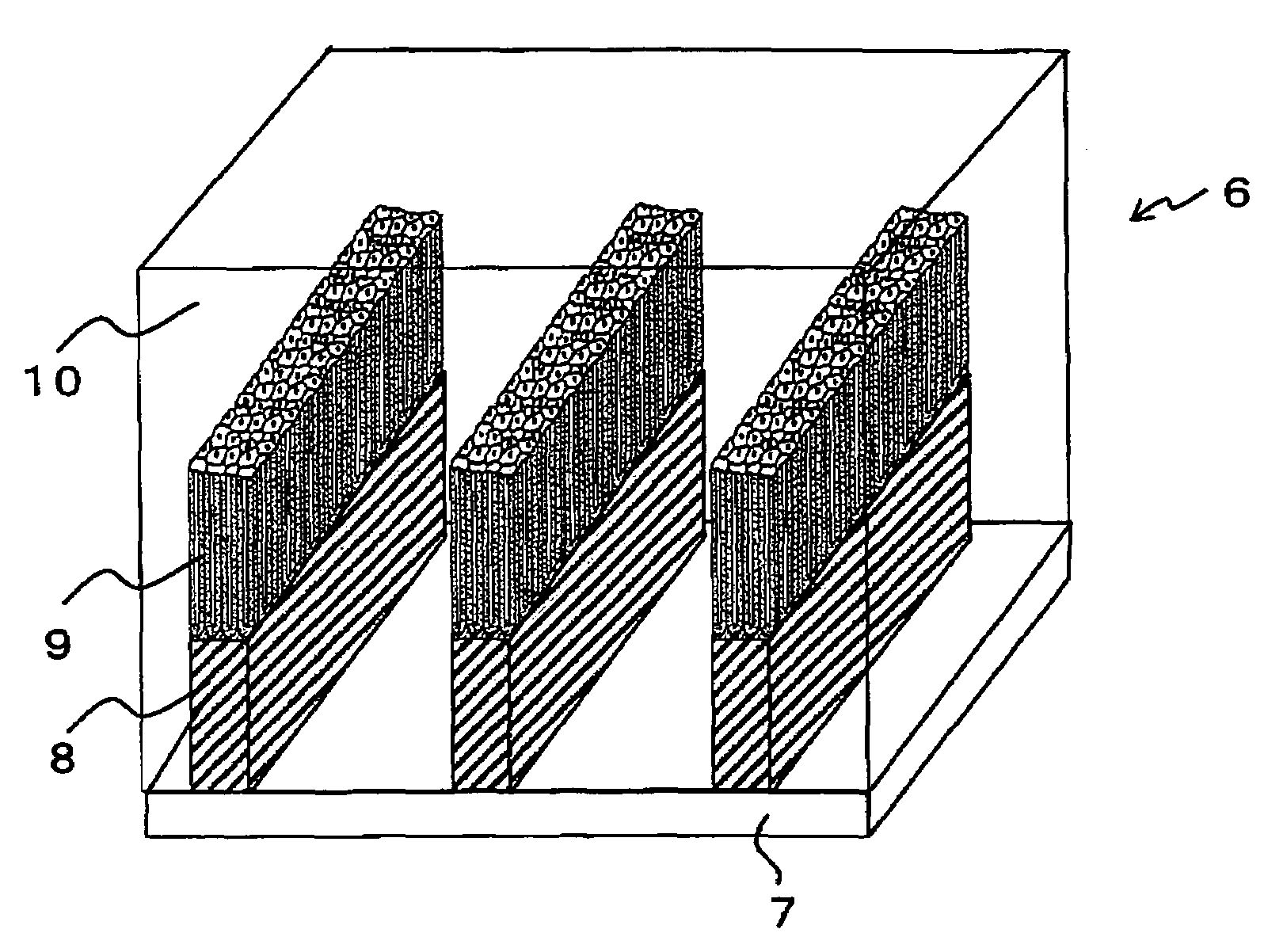
[0055]FIG. 2 illustrates a polarizing optical device 6 according to a second embodiment of the present invention. The polarizing optical device 6 may include a substrate 7 and an extrafine grid structure 8 at one major surface of the substrate 7. The extrafine grid structure 8 may include a porous compound metal part 9. The porous compound metal part 9 may be colored to further enhance the anti-reflection characteristics of the polarizing optical device 6.
[0056]For example, when the extrafine grid structure 8 is aluminum, the porous compound metal part 9 may be a porous aluminum oxide film, i.e., an alumite film. The porous aluminum oxide film may be formed, e.g., by an anodic oxidation process, i.e., an alumite process.
[0057]The substrate 7 may be, e.g., optically transparent glass or resin film, such as PET, PC, or PMMA. A height, a wire width, a wire distance, and an average grid pitch of the extrafine grid structure 8 may be about, e.g., 300 nm, 50 nm, 100 nm, and 150 nm, respec...
third embodiment
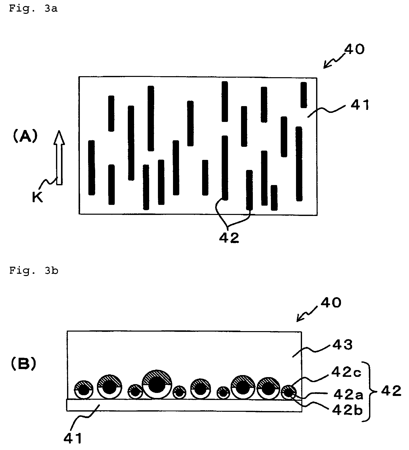
[0073]FIGS. 3a and 3b illustrate a polarizing optical device 40 according to a third embodiment of the present invention. Specifically, FIG. 3a illustrates a plan schematic view of the polarizing optical device 40, and FIG. 3b illustrates a cross-sectional view of the polarizing optical device 40.
[0074]The polarizing optical device 40 may include a plurality of unit constituents 42 disposed at one major surface of a substrate 41 in a dispersed fashion. Each unit structural member 42 may be formed by coating one half side of a carbon nano tube 42a with a metal 42b, e.g., aluminum. The carbon nano tubes 42b may be arranged in a predetermined direction (in a direction indicated by an arrow K in FIG. 3a). Also, a porous compound metal part 42c, e.g., an alumite film, may be formed at the other half side of each carbon nano tube 42a, which is exposed to the air, by, e.g., an anodic oxidation process (an alumite process). Specifically, the porous compound metal part 42c may be colored as ...
PUM
| Property | Measurement | Unit |
|---|---|---|
| light transmittance | aaaaa | aaaaa |
| diagonal size | aaaaa | aaaaa |
| height | aaaaa | aaaaa |
Abstract
Description
Claims
Application Information


