Insulating layer between bumps of semiconductor chip, and display panel using the same with anisotropic conductive film between semiconductor chip and substrate

a technology of semiconductor chips and bumps, applied in semiconductor devices, semiconductor/solid-state device details, electrical devices, etc., can solve the problem of raising the price of raw materials of acf, and achieve the effect of improving the remaining ratio of conductive particles

Active Publication Date: 2010-07-06
SAMSUNG DISPLAY CO LTD
View PDF15 Cites 42 Cited by
  • Summary
  • Abstract
  • Description
  • Claims
  • Application Information

AI Technical Summary

Benefits of technology

[0014]An exemplary embodiment of the present invention provides a semiconductor chip and manufacturing method thereof which may improve the remaining ratio of conductive particles of an ACF, and a display panel using the semiconductor chip and manufacturing method thereof.

Problems solved by technology

Although a method of increasing the amount of conductive particles contained in the ACF may be considered in order to increase the remaining ratio of the conductive particles under the bump, this method raises the price of raw materials of the ACF.

Method used


Image

  • Insulating layer between bumps of semiconductor chip, and display panel using the same with anisotropic conductive film between semiconductor chip and substrate
  • Insulating layer between bumps of semiconductor chip, and display panel using the same with anisotropic conductive film between semiconductor chip and substrate
  • Insulating layer between bumps of semiconductor chip, and display panel using the same with anisotropic conductive film between semiconductor chip and substrate

Examples


Embodiment Construction

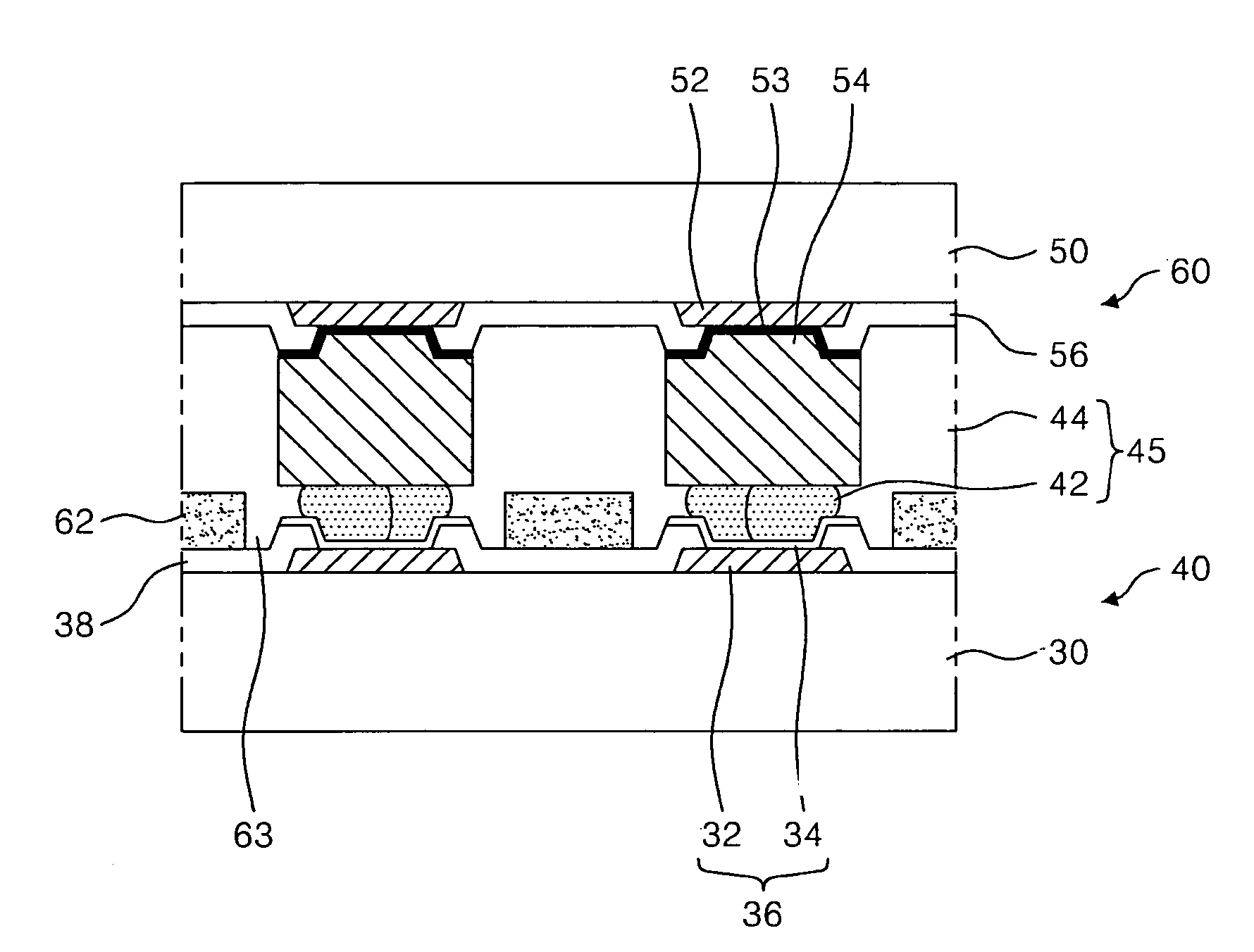
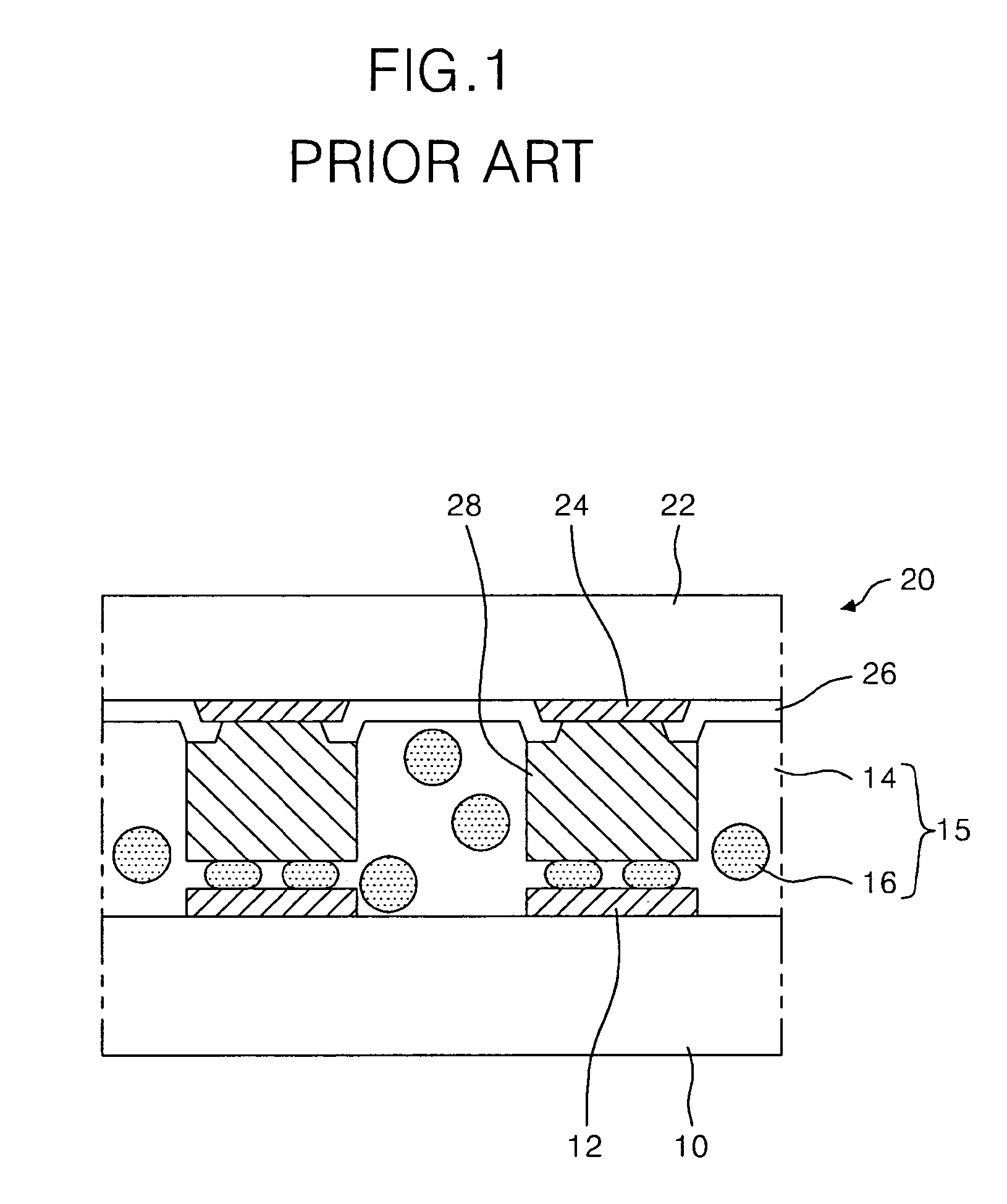
[0036]The invention is described more fully hereinafter with reference to the accompanying drawings, in which exemplary embodiments of the invention are shown. This invention may, however, be embodied in many different forms and should not be construed as limited to the exemplary embodiments set forth herein. Rather, these embodiments are provided so that this disclosure will be thorough and complete, and will fully convey the scope of the invention to those skilled in the art. In the drawings, the size and relative sizes of layers and regions may be exaggerated for clarity.

[0037]It will be understood that when an element or layer is referred to as being “on” or “connected to” another element or layer, the element or layer can be directly on or connected to another element or layer or intervening elements or layers. In contrast, when an element is referred to as being “directly on” or “directly connected to” another element or layer, there are no intervening elements or layers prese...


PUM


Abstract

A semiconductor chip and manufacturing method thereof, the semiconductor chip including a plurality of bumps connected to a driving circuit integrated on a semiconductor substrate and an organic insulating layer disposed on the driving circuit. The organic insulating layer extends from the semiconductor substrate less than the plurality of bumps such that a lower edge of the plurality of bumps protrudes further than a lower edge of the organic insulating layer.

Description

[0001]This application claims priority to Korean Patent application No. 2005-0077657 filed on Aug. 24, 2005, and all the benefits accruing therefrom under 35 U.S.C. §119, the contents of which are herein incorporated by reference in its entirety.BACKGROUND OF THE INVENTION[0002]1. Field of the Invention[0003]The present invention relates to a semiconductor chip and display panel using the same, and more particularly, to a semiconductor chip and manufacturing method thereof which can improve the remaining ratio of anisotropic conductive particle, and a display panel using the semiconductor chip and manufacturing thereof.[0004]2. Description of the Related Art[0005]As flat panel displays, which are popular as a display device, there are a liquid crystal display (LCD) using a liquid crystal, a plasma display panel (PDP) using a discharge of an inert gas, and an organic electroluminescent display (OLED) using an organic light emitting diode. Among these displays, the PDP is applied to l...

Claims


Application Information

Patent Timeline
Patent Type & Authority Patents(United States)
IPC IPC(8): H01L23/48H01L21/00
CPCH01L23/3171H01L24/11H01L24/13H01L24/29H01L24/12H01L24/16H01L24/17H01L24/83H01L2924/12041H01L2924/00013H01L2224/293H01L2224/2929H01L2224/81903H01L2924/01006H01L2224/83851H01L2224/13016H01L2924/19041H01L2924/12044H01L2924/0781H01L2924/01082H01L2924/01079H01L2924/01042H01L2924/01033H01L2224/114H01L2224/116H01L2224/13012H01L2224/13099H01L2224/13144H01L2224/16H01L2224/83136H01L2224/83192H01L2224/838H01L2924/01002H01L2924/01004H01L2924/01013H01L2924/01022H01L2924/00014H01L2224/29099H01L2224/29199H01L2224/29299H01L2924/00H01L2224/05124H01L2224/05144H01L2224/05155H01L2224/05572H01L2224/05666H01L2224/0615H01L2224/10145H01L2224/10175H01L2224/11H01L2224/13
Inventor CHO, WON GUKANG, HO MIN
Owner SAMSUNG DISPLAY CO LTD
Why Eureka
Try Eureka