However, FPGAs typically occupy between 20 and 40 times the surface area of
semiconductor or
footprint than an equivalent standard-
cell ASIC, have poorer power and circuit speed performance, offer fewer
degrees of freedom for user customisation, provide a smaller number of gates available for implementation, and are also considerably more expensive on a per-unit basis.
However, the cost of initially developing a new customised ASIC is extremely high, and such non-recurring
engineering (NRE) costs make ASICs attractive only when produced in high volumes so that the NRE costs can be absorbed without appreciably increasing the cost per unit, or when the number of gates required exceeds the capacity of an FPGA, or when specialised functionality not available in an FPGA is required, or when high speed or low power operation is required and cannot be achieved with an FPGA.
However, the translation process is not straightforward and can be excessively
time consuming and costly.
Moreover, structural differences between FPGA and ASIC circuit components and interconnects can cause the FPGA and ASIC implementations of the final circuit to behave differently, which greatly complicates the translation process.
Further, as FPGAs are unable to provide as many gates as ASICs, such an approach necessarily limits the number of gates that can be so prototyped.
A possible
workaround is to use multiple FPGAs for prototyping and a single ASIC for production; however, this even further complicates the translation process.
Moreover, multiple FPGAs in a prototype
system cannot be readily substituted with an ASIC due to the difference in form factor of their respective packages.
(Some structured ASICs can also be effectively “customized” through the use of programmable lookup tables which reside in the logic fabric; however, the physical implementation of the lookup tables is fixed and cannot be altered.)
However, despite the many advantages of structured
ASIC technology, the development of new prototype circuits nevertheless requires one or more new routing layer and / or via masks to be developed, and this can be
time consuming, prone to error, and expensive.
Maskless technologies that use e-beam or other approaches to customise the routing have been developed as an alternative, but are an expensive and
time consuming method of customising interconnect compared to traditional FPGAs.
None of these techniques are readily available in the case of ASICs due to the high cost and manufacturing time associated with ASIC prototype production.
Due to the potentially larger size and complexity of ASICs and the lack of availability of the above techniques, ASICs are consequently much more difficult to debug than FPGAs.
Since ASICs lack reprogrammability, the traditional ASIC approach typically requires compromises to be made in providing the physical die resources necessary to ensure that a device can be tested and debugged sufficiently to verify the
correctness of the design.
However, the approach whereby external input and output pins provide the means of testing the device is necessarily limited by the degree of
controllability and
observability that the external pins are able to provide.
Further difficulty often exists in providing the necessary capability in the external means of control and observation to provide the degree of control and observation required to perform design
verification.
This is due to the speed and complexity of the necessary device stimuli and response behaviour, hence the provision of external means of control and observation having the desired degree of complexity and performance is usually complex and expensive.
The addition of test-specific logic components for
testability necessarily imposes an overhead on both the
design process and device manufacture because such components are designed prior to device fabrication, require additional
semiconductor die area, and themselves need to be verified and tested as with the other circuitry of the device.
The state of the art in integrated circuit production is constantly evolving with such devices becoming more complex, operating at higher speeds, and incorporating an increasing amount of circuitry in a single device.
The addition of internal
connectivity and test-specific logic functionality to ASICs is a useful approach for enhancing
testability, but is wasteful of semiconductor die area and introduces unwanted complexity into the
design process.
This manufacturing process is costly and does not provide the quick turn-around time that is required to match the debugging capabilities of FPGAs.
However, they are also more complex and expensive to design, very expensive and slow to prototype, require detailed consideration of more factors (e.g.,
clock distribution), and are more difficult to debug.
Structured ASICs attempt to provide a compromise between ASICs and FPGAs; however they still lack the reprogrammability that makes FPGAs attractive: the capability to be entirely reprogrammed without going through a physical manufacturing process.
Another significant
disadvantage of structured ASICs compared to FPGAs is that because they must go through a physical manufacturing process in order to be customized or “programmed” for use, they cannot be offered to customers as a standard component.


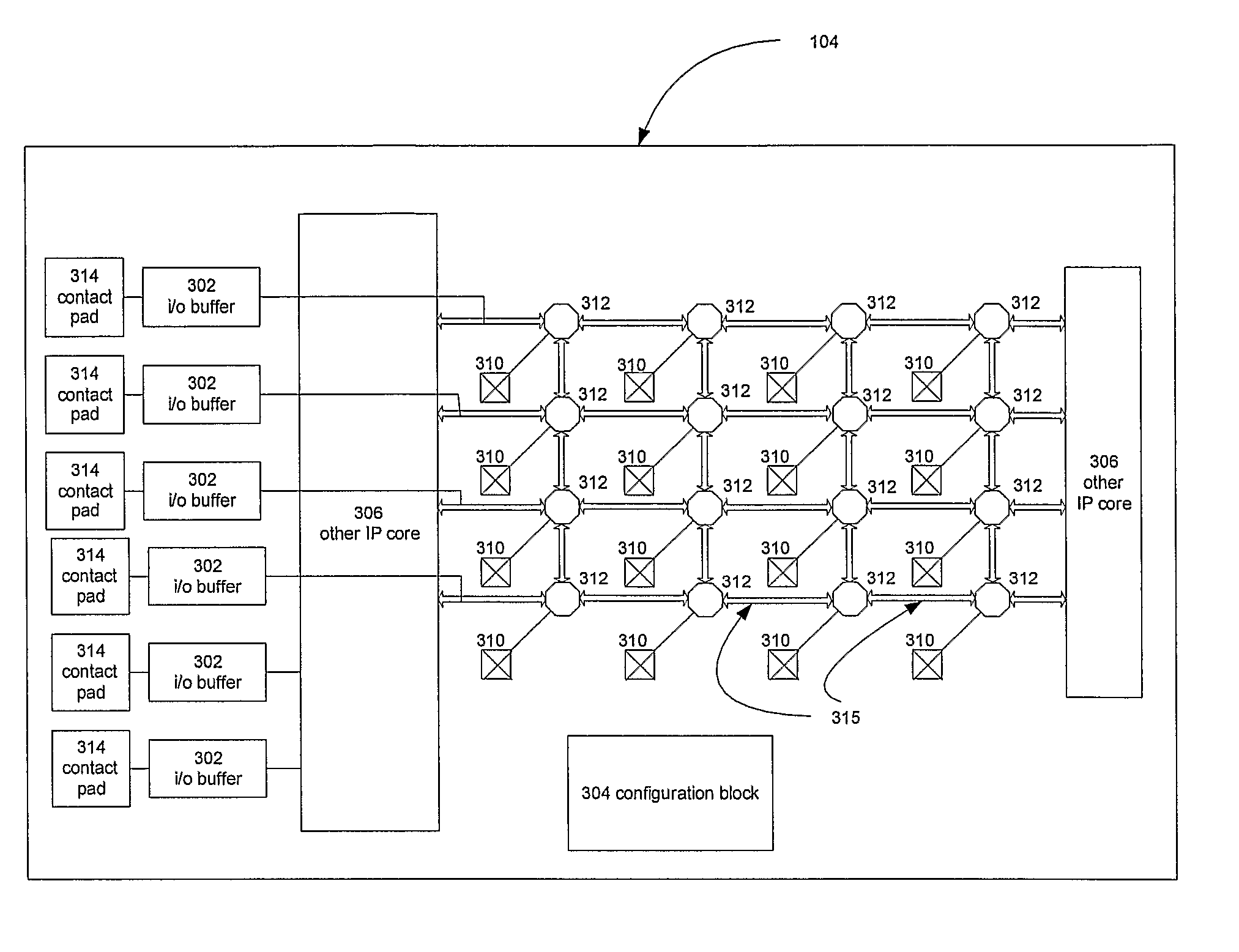
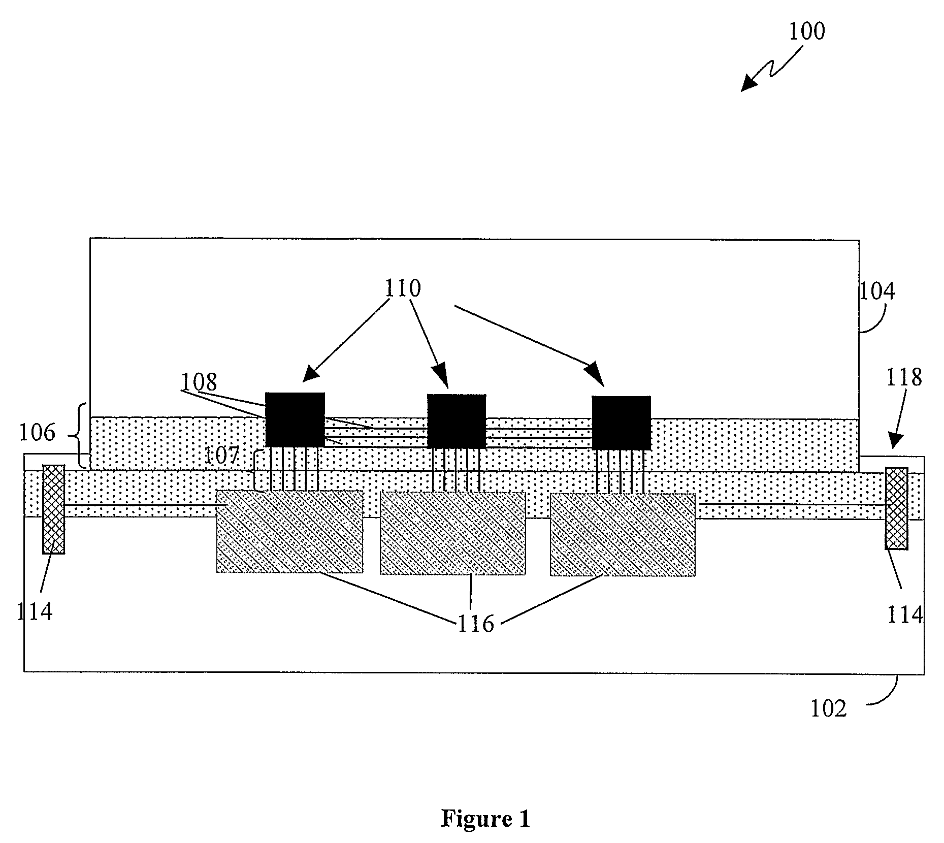
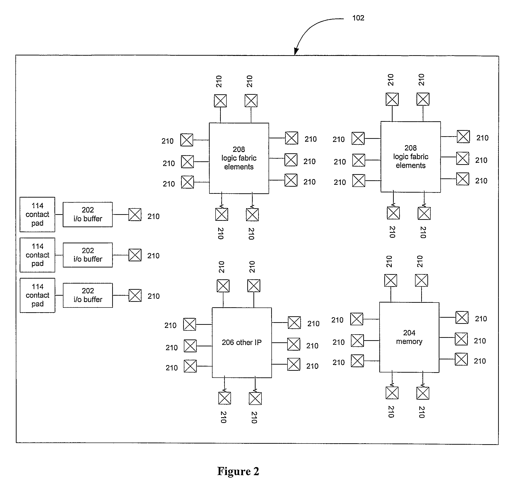