Half-tone type phase-shifting mask and method for manufacturing the same
a phase-shifting mask and half-tone technology, applied in the field of photomasks, can solve the problems of increasing the mark of the photolithographic step applied in the manufacturing process of semiconductors, and achieve the effect of improving the mark of the photolithographic step
- Summary
- Abstract
- Description
- Claims
- Application Information
AI Technical Summary
Benefits of technology
Problems solved by technology
Method used
Image

Examples
first embodiment
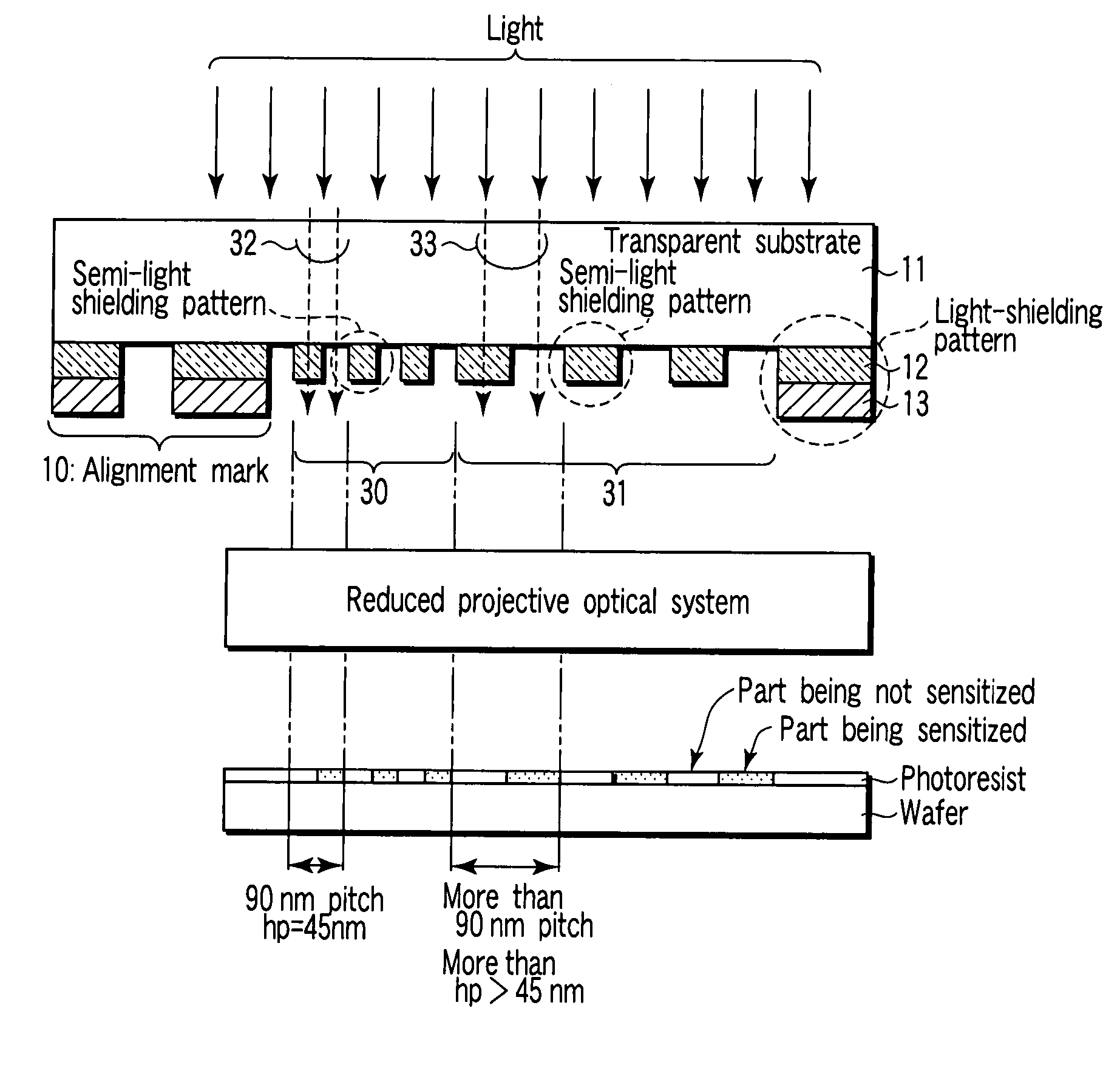
[0038]FIG. 1 is a diagram showing a half-tone type phase-shifting mask according to a first embodiment of the present invention.
[0039]As shown in FIG. 1, the half-tone type phase-shifting mask in the embodiment is provided with a transparent substrate 11, a half-tone film 12, and a light-shielding film 13. The half-tone film 12 is provided on an area in which a light-shielding pattern is formed and another area in which a semi-light shielding pattern is formed in the transparent substrate 11. The light-shielding film 13 is provided on an area in which the light-shielding pattern is formed in the half-tone film 12. An example of the light-shielding pattern is a light-shielding belt section provided in a photomask for suppressing a leaking light at the time of exposing a wafer.
[0040]The semi-light shielding pattern includes a first semi-light shielding pattern 31 composed of the half-tone film 12, and a second semi-light shielding pattern 30 composed similarly of the half-tone film 12...
second embodiment
[0065]A second embodiment is another example of the processing steps for achieving a high transmittance described in the first embodiment. In the second embodiment, the processing steps for achieving high transmittance are conducted such that mask blanks on the way to processing are subjected to heat treatment for one hour at 450° C. in the atmospheric environment by using a mask substrate heat-treating device.
[0066]Although the atmosphere is not specifically limited, when it is the atmospheric air or an oxygen atmosphere, oxidation is promoted in the surface of the half-tone film 12 so that it is effective for elevating transmittance. Thus, a light transmittance of the half-tone film 12 in the region in which the surface is exposed increases from 2% to 4%. It is to be noted that the light transmittance of the region the surface of which is covered with the light-shielding film (for example, chromium film) 13 in the half-tone film 12 is still 2%.
[0067]As described above, a light tra...
third embodiment
[0068]A third embodiment is a further example of the processing steps for achieving high transmittance described in the first embodiment as in the second embodiment.
[0069]In the third embodiment, the processing steps for achieving a high transmittance are implemented by a plasma treatment which is carried out with the use of a dry etching device for mask in conditions of a power=200 W, a pressure=20 mT, and an oxygen flow rate=100 sccm for thirty minutes. Although oxygen gas is used in this case, effects of high transmittance due to the same surface reforming can be obtained also by using hydrogen, helium, nitrogen and the like as plasma.
[0070]In the present example, although a case where surface reforming effects are sought without etching a half-tone pattern has been mentioned, realization of high transmittance is also possible by removing a part of the surface by means of plasma etching. In this case, gases to be used for the plasma, and the plasma conditions are not specifically...
PUM
| Property | Measurement | Unit |
|---|---|---|
| light transmittance | aaaaa | aaaaa |
| light transmittance | aaaaa | aaaaa |
| thickness | aaaaa | aaaaa |
Abstract
Description
Claims
Application Information
 - R&D
- Intellectual Property
- Life Sciences
- Materials
- Tech Scout
- Unparalleled Data Quality
- Higher Quality Content
- 60% Fewer Hallucinations
Browse by: Latest US Patents, China's latest patents, Technical Efficacy Thesaurus, Application Domain, Technology Topic, Popular Technical Reports.
© 2025 PatSnap. All rights reserved.Legal|Privacy policy|Modern Slavery Act Transparency Statement|Sitemap|About US| Contact US: help@patsnap.com