Supercharge Your Innovation With Domain-Expert AI Agents!

Semiconductor device with gate dielectric containing aluminum and mixed rare earth elements

a technology of rare earth elements and semiconductor devices, which is applied in the direction of coatings, capacitors, chemical vapor deposition coatings, etc., can solve the problems of reduced channel mobility, large densities of interface traps, and various problems of current high-k dielectric materials under evaluation

Inactive Publication Date: 2010-07-20
TOKYO ELECTRON LTD
View PDF39 Cites 14 Cited by
  • Summary
  • Abstract
  • Description
  • Claims
  • Application Information

AI Technical Summary

Benefits of technology

These mixed rare earth based films offer enhanced thermal stability, increased dielectric constants, reduced interface trap densities, and improved processing characteristics, addressing the limitations of existing high-k dielectric materials for future semiconductor applications.

Problems solved by technology

Current high-k dielectric materials under evaluation suffer from various problems.
Some of the problems encountered include film crystallization during anneals, growth of interfacial layers during deposition and further processing, large densities of interface traps, reduced channel mobility, reaction with poly-silicon gates, and Fermi level pinning with metal gates.
Other problems encountered with current high-k dielectric materials include dielectric constants that are too low compared to desired values for advanced semiconductor devices.

Method used


Image

  • Semiconductor device with gate dielectric containing aluminum and mixed rare earth elements
  • Semiconductor device with gate dielectric containing aluminum and mixed rare earth elements
  • Semiconductor device with gate dielectric containing aluminum and mixed rare earth elements

Examples


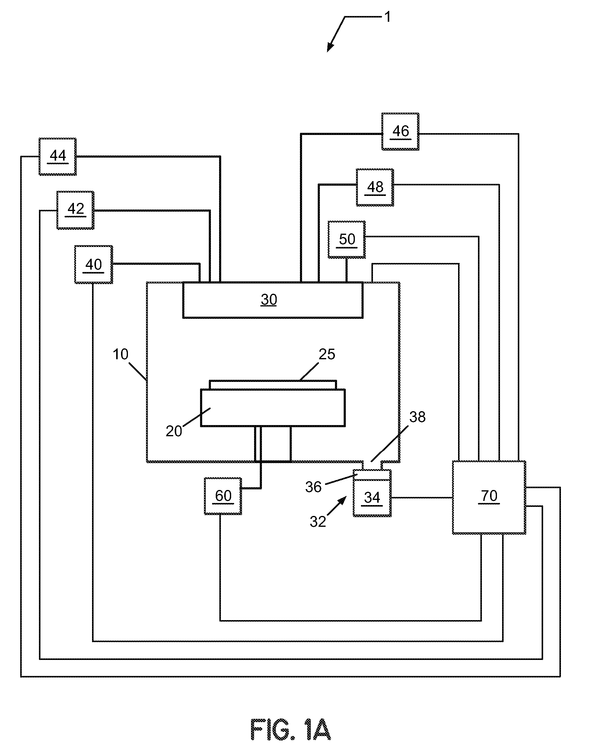
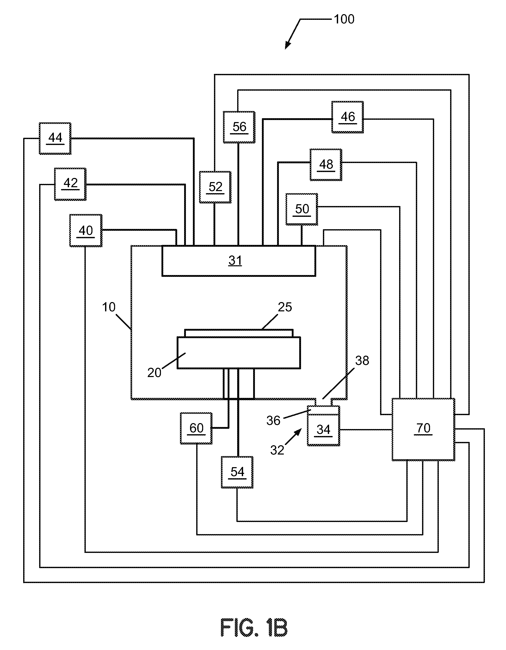
Embodiment Construction

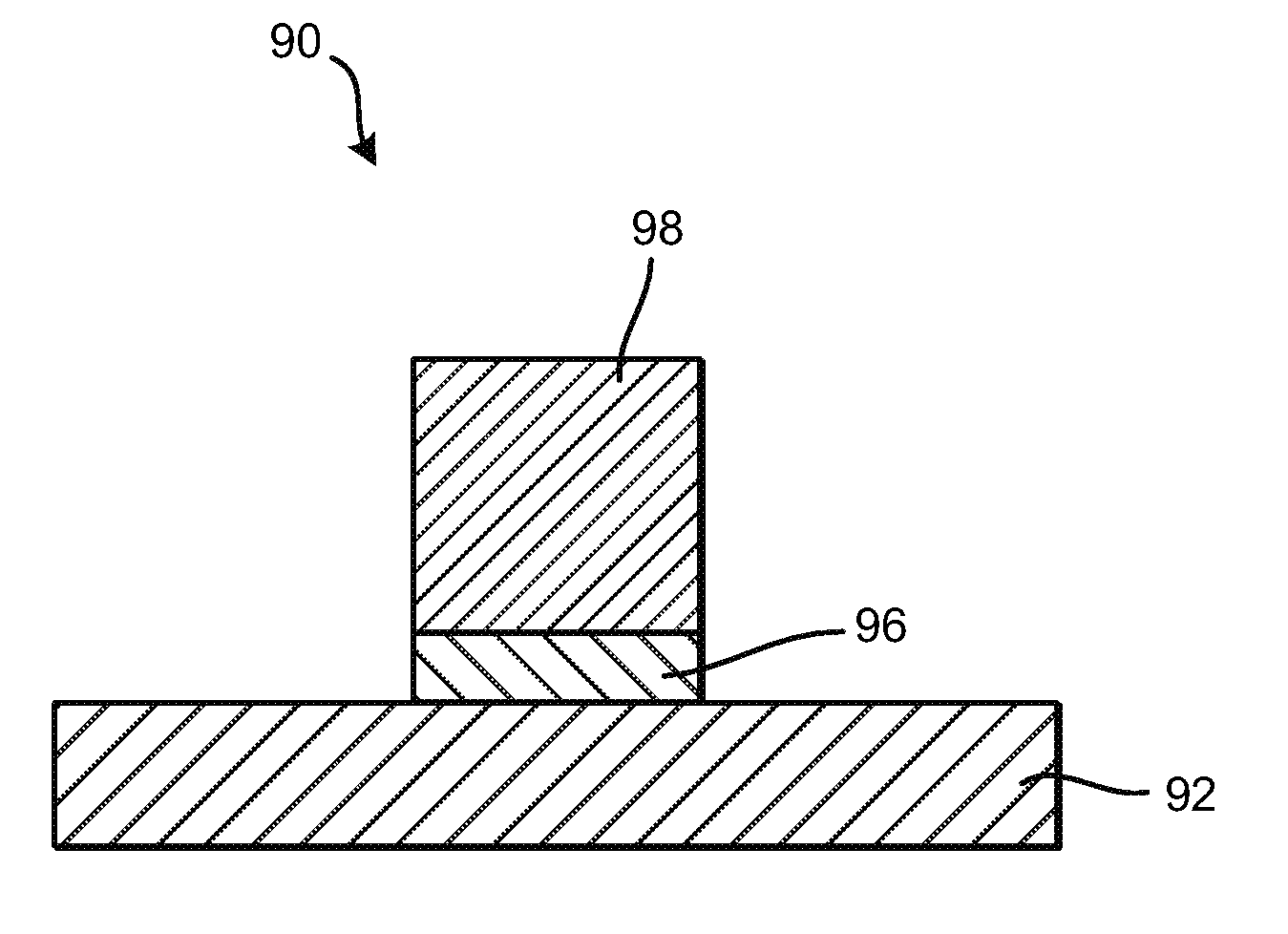
[0024]As in the case of mixed Zr / Hf oxide based materials, mixed rare earth based materials are likely to provide beneficial thermal and electrical characteristics for future high-k applications in semiconductor applications. As used herein, mixed rare earth based materials refer to materials containing a plurality of, i.e., at least two, different rare earth metal elements. Because the rare earth elements are chemically similar and practically infinitely miscible as oxides, nitrides, oxynitrides, aluminates, aluminum nitrides, and aluminum oxynitrides, they are expected to form highly stable solid solutions with other rare earth elements. Expected benefits of a film containing a mixed rare earth based material incorporating a plurality of rare earth metal elements include increased thermal stability in contact with silicon or metal gate electrode material, increased crystallization temperature, increased dielectric constant compared to rare earth based materials containing a single...


PUM

PropertyMeasurementUnit
thicknessaaaaaaaaaa
thicknessaaaaaaaaaa
temperatureaaaaaaaaaa

Abstract

A semiconductor device, such as a transistor or capacitor, is provided. The device includes a substrate, a gate dielectric over the substrate, and a conductive gate electrode film over the gate dielectric. The gate dielectric includes a mixed rare earth aluminum oxide, nitride or oxynitride film containing aluminum and at least two different rare earth metal elements.

Description

CROSS-REFERENCE TO RELATED APPLICATIONS[0001]This application is related to co-pending U.S. patent application Ser. No. 11 / 278,387, entitled “METHOD OF FORMING MIXED RARE EARTH OXIDE AND ALUMINATE FILMS BY ATOMIC LAYER DEPOSITION,” filed on even date herewith; co-pending U.S. patent application Ser. No. 11 / 278,393, entitled “METHOD OF FORMING MIXED RARE EARTH NITRIDE AND ALUMINUM NITRIDE FILMS BY ATOMIC LAYER DEPOSITION,” filed on even date herewith; co-pending U.S. patent application Ser. No. 11 / 278,396, entitled “METHOD OF FORMING MIXED RARE EARTH OXYNITRIDE AND ALUMINUM OXYNITRIDE FILMS BY ATOMIC LAYER DEPOSITION,” filed on even date herewith; and co-pending U.S. patent application Ser. No. 11 / 278,397, entitled “SEMICONDUCTOR DEVICE WITH GATE DIELECTRIC CONTAINING MIXED RARE EARTH ELEMENTS,” filed on even date herewith. The entire contents of these applications are herein incorporated by reference in their entirety.FIELD OF INVENTION[0002]The present invention relates to a dielec...

Claims


Application Information

Patent Timeline
Patent Type & Authority Patents(United States)
IPC IPC(8): H01L29/94
CPCC23C16/303C23C16/308C23C16/403H01L21/28194H01L21/3141H01L28/40H01L29/517H01L29/78H01L29/94H01L21/02192H01L21/0228H01L21/02194H01L21/02274H01L21/02178
Inventor CLARK, ROBERT D.
Owner TOKYO ELECTRON LTD
Features
  • R&D
  • Intellectual Property
  • Life Sciences
  • Materials
  • Tech Scout
  • Unparalleled Data Quality
  • Higher Quality Content
  • 60% Fewer Hallucinations
Learn More