Supercharge Your Innovation With Domain-Expert AI Agents!

Particle inspection apparatus, exposure apparatus, and device manufacturing method

a technology of exposure apparatus and inspection apparatus, applied in the direction of photomechanical apparatus, instruments, originals for photomechanical treatment, etc., can solve the problems of reducing the operating rate of the exposure apparatus, difficult to avoid all diffract light, and low manufacturing yield of ics or lsis, so as to reduce the detection error

Inactive Publication Date: 2010-07-20
CANON KK
View PDF12 Cites 3 Cited by
  • Summary
  • Abstract
  • Description
  • Claims
  • Application Information

AI Technical Summary

Benefits of technology

This approach reduces detection errors and maximizes the operating rate of exposure apparatuses by accurately distinguishing between particle scattering light and pattern diffracted light, thereby optimizing the inspection process.

Problems solved by technology

This lowers manufacturing yields of ICs or LSIs.
However, since the integration density of ICs has been increased and the circuit pattern has been diversified in recent years, it is difficult to avoid all diffracted light 34 by simply adjusting the positions of the image sensors 19a and 19b.
This reduces the operating rate of the exposure apparatus.

Method used


Image

  • Particle inspection apparatus, exposure apparatus, and device manufacturing method
  • Particle inspection apparatus, exposure apparatus, and device manufacturing method
  • Particle inspection apparatus, exposure apparatus, and device manufacturing method

Examples


Embodiment Construction

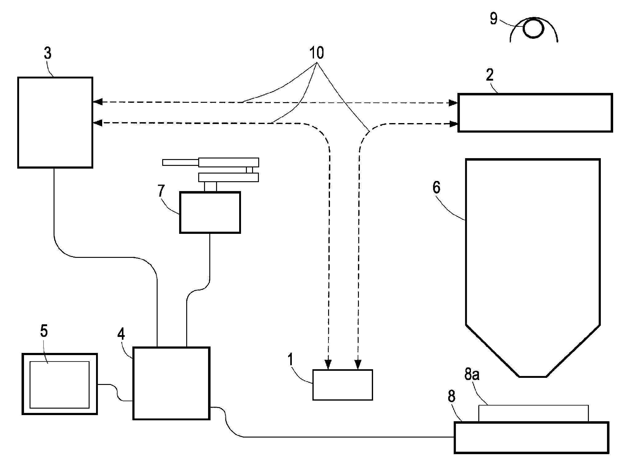
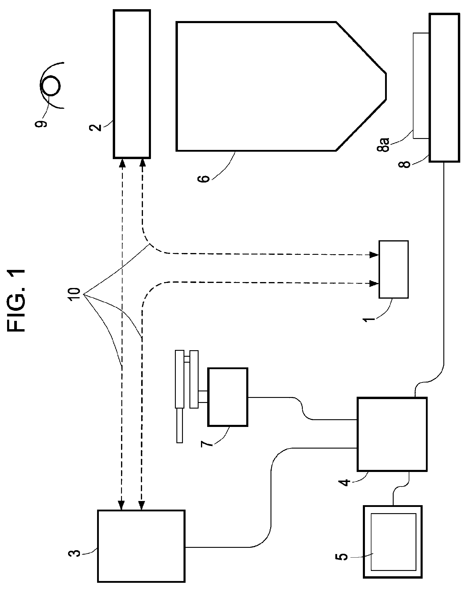
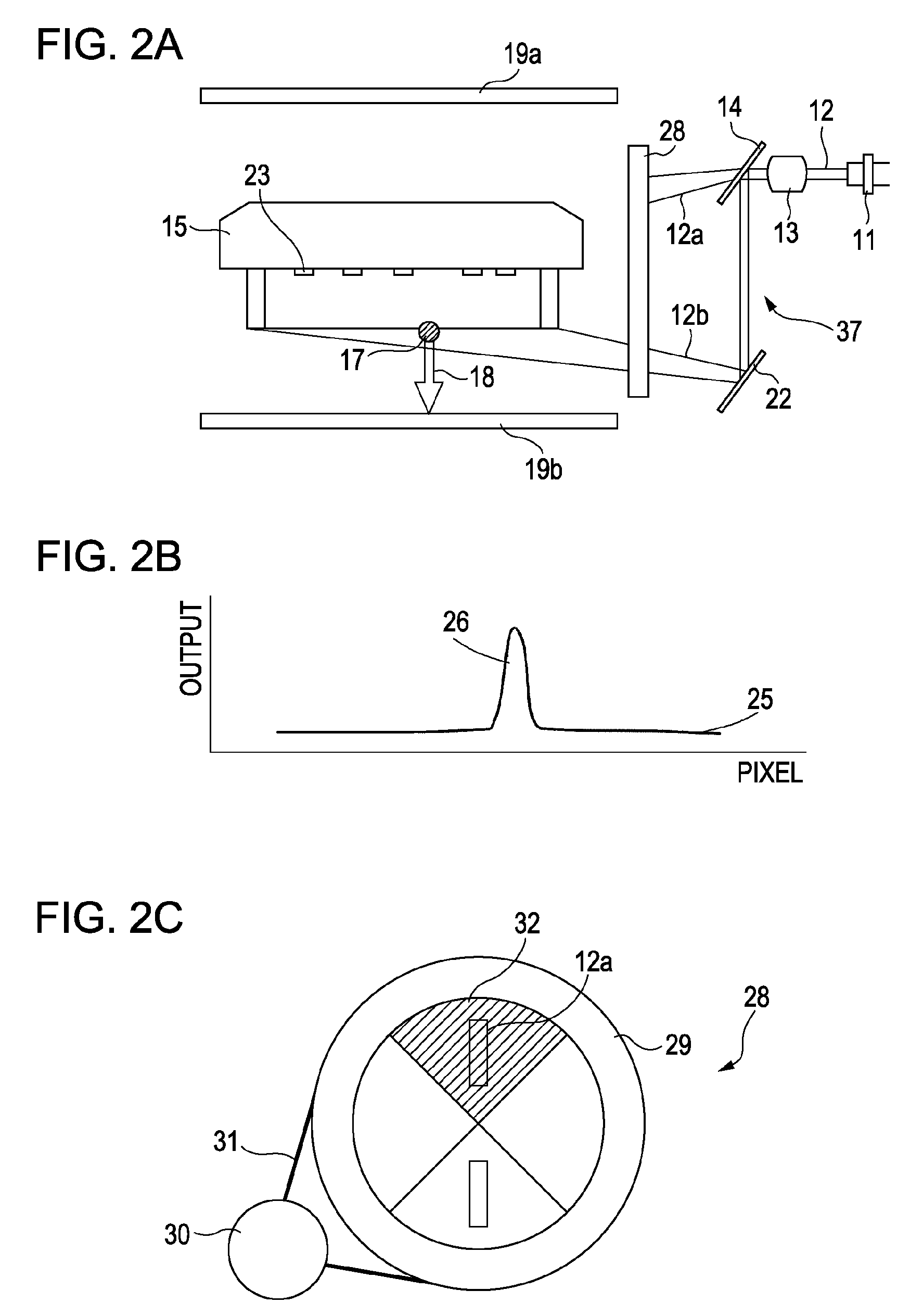
[0039]A semiconductor exposure apparatus including a particle inspection apparatus according to an embodiment of the present invention will be described with reference to FIG. 1.

[0040]The semiconductor exposure apparatus according to this embodiment repeatedly transfers a circuit pattern in multiple shot regions on a wafer by a step-and-repeat method using an exposure original, such as a reticle or a photomask, which is used in the semiconductor field.

[0041]A reticle serving as an original is first placed at a reticle insertion port 1. A reticle stage 2 is a mechanism for holding the reticle above a projection lens 6.

[0042]A particle inspection apparatus 3 according to this embodiment makes an inspection for adhesion of a particle to the reticle. A control device 4 controls a conveying robot, which will be described below, gives the particle inspection apparatus 3 instructions to convey the reticle and to conduct a particle inspection, and controls exposure.

[0043]A console 5 allows ...


PUM

PropertyMeasurementUnit
thresholdaaaaaaaaaa
surface-aaaaaaaaaa
integration densityaaaaaaaaaa

Abstract

A particle inspection apparatus includes an irradiation unit configured to apply a light beam onto front and back surfaces of an object to be inspected, first and second detection units configured to detect scattering light from the surfaces, a calculation unit configured to conduct a particle inspection on the surfaces on the basis of outputs from the detection units, and a control unit configured to control the irradiation unit, the detection units, and the calculation unit. The irradiation unit can selectively apply the beam onto the front or back surface. The control unit causes the calculation unit to conduct the particle inspection on the inspection surface on which the light beam is selectively applied, on the basis of outputs made by the detection unit corresponding to simultaneous application and selective application of the light beam.

Description

BACKGROUND OF THE INVENTION[0001]1. Field of the Invention[0002]The present invention relates to a particle inspection apparatus that detects a particle adhering to an object to be inspected, for example, an original.[0003]2. Description of the Related Art[0004]In exposure apparatuses, a circuit pattern used to manufacture a device, for example, a semiconductor device such as an IC or an LSI, a CCD, a liquid crystal panel, or a magnetic head (hereinafter generically named a “device”) is provided on an original called a reticle or a photomask.[0005]A pellicle serving as a protective cover is attached to an original so as to prevent a particle from adhering onto the original.[0006]In a normal IC manufacturing process, a circuit pattern provided on an original, such as a reticle or a photomask, is transferred onto a resist-coated wafer by an exposure apparatus (stepper or mask aligner).[0007]In this case, if a particle, such as a pattern defect or dust, is present on the original, the ...

Claims


Application Information

Patent Timeline
Patent Type & Authority Patents(United States)
IPC IPC(8): G01N21/88G01N21/956G03F1/84G03F7/20H01L21/027
CPCG03F1/0092G03F1/84G03F7/7065G03F7/70908G03F1/68G03F7/706851
Inventor KAWAHARA, ATSUSHI
Owner CANON KK
Features
  • R&D
  • Intellectual Property
  • Life Sciences
  • Materials
  • Tech Scout
  • Unparalleled Data Quality
  • Higher Quality Content
  • 60% Fewer Hallucinations
Learn More