Copolymer for charge transport layer in opto-electronic device

a technology of optoelectronic devices and copolymers, which is applied in the direction of natural mineral layered products, layered products, chemistry apparatuses and processes, etc., can solve the problem of not and achieve the reduction of ppv derivatives can be enhanced, and the effect of reducing the solubility of polymers

Inactive Publication Date: 2010-08-03
KONINKLIJKE PHILIPS ELECTRONICS NV
View PDF12 Cites 2 Cited by
  • Summary
  • Abstract
  • Description
  • Claims
  • Application Information

AI Technical Summary

Benefits of technology

[0009]It has been demonstrated that charge transport in e.g. PPV derivatives can be enhanced by the use of long symmetrical side-chains. However, applying long symmetrical side chains does not reduce the solubility of the polymer. Reduction of the solubility can be achieved by addition of monomers with symmetrical short side chains. This can surprisingly be done without jeopardizing the enhanced charge transport properties. Consequently, the solubility in a first solvent can be continuously adjusted by a tuning of the mutual ratio of the monomers having long and short (symmetrical) side chains, while preserving the enhanced charge transport properties and the solubility in a second solvent. In this way, a charge transport layer can be chosen to have lower solubility in a first solvent than the highly luminescent LEP layer in the same first solvent. This charge transport layer, with limited solubility in a first solvent, can be spin cast in a second solvent and can then be easily combined with a thin, highly luminescent layer spin cast with the first solvent.
[0013]The copolymers of the invention may easily be selected from the group of compounds comprising mixtures of two or more monomers and? homopolymers with a solubility ratio in a first solvent of at least 10.

Problems solved by technology

However, applying long symmetrical side chains does not reduce the solubility of the polymer.

Method used


Image

  • Copolymer for charge transport layer in opto-electronic device
  • Copolymer for charge transport layer in opto-electronic device
  • Copolymer for charge transport layer in opto-electronic device

Examples


Embodiment Construction

[0018]Although the preferred embodiments relate to a light-emitting device (LED), the copolymer of the invention may be used in other opto-electrical devices comprising more than one layer of a conjugated polymer.

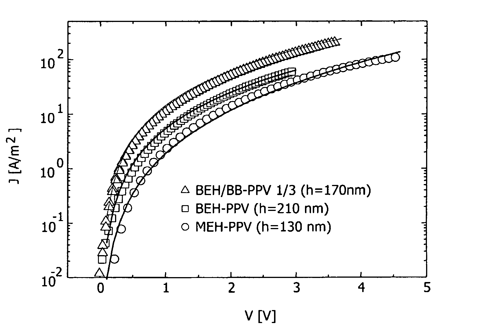
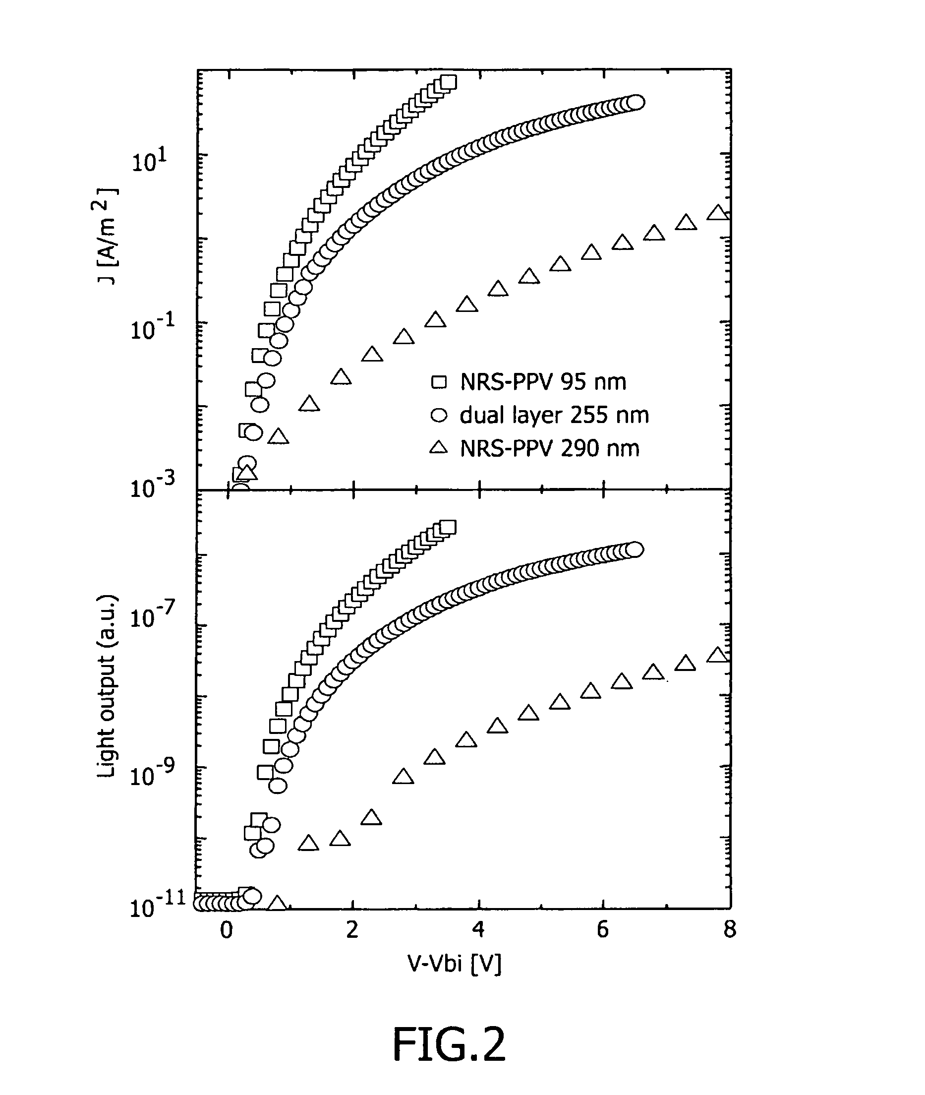
[0019]Polymer synthesis: MEH-PPV, BEH-PPV, and BEH / BB-PPV ⅓ were synthesized according to the procedure of MEH-PPV in the presence of 0.5-1.0% of 4-methoxyphenol, by Neef et al. in Macromolecules 2000, 33, 2311. The structures of the polymers used are shown below. The precursors were carefully purified by crystallization (3×) and the obtained polymers were purified by a second precipitation from acetone. NRS-PPV has been synthesized according to the procedure indicated in Adv. Mater. 1998, 10, 1340.

[0020]Polymer analysis: Molecular weights were determined by gel permeation chromatography (GPC); they were measured in trichlorobenzene at 135° C. and calibrated with polystyrene standards.

[0021]

[0022]The combination of BEH-PPV and BB-PPV in various ratios in copolymers can indu...


PUM

PropertyMeasurementUnit
areaaaaaaaaaaa
areaaaaaaaaaaa
temperatureaaaaaaaaaa

Abstract

The invention relates to a copolymer for a charge transport layer in an optoelectronic device and in particular in a light-emitting diode (LED), having a charge mobility of at least 1.0×10¹⁰ m2 / V.s, and comprising at least a first and a second monomer, characterized in that the ratio of the solubilities of homopolymers made from the first and the second monomer in a first solvent is more than 10. This copolymer allows a (semi) conductive polymer to be cast to form a first layer and prevents it from being dissolved in the solvent of a subsequently deposited second, e.g. light-emitting layer. The invention further relates to a LED comprising a copolymer according to the invention.

Description

FIELD OF THE INVENTION[0001]The invention relates to a copolymer for a charge transport layer in an opto-electronic device and in particular in an electroluminescent device comprising an anode, a cathode, a light-emitting layer, and at least one charge transport layer. An opto-electronic device is understood to be any device that functions as an electrical-to-optical or optical-to-electrical transducer, or an instrument that uses such a device in its operation. Photodiodes, photodetectors, light-activated switches, electroluminescent devices (LEDs), injection laser diodes, and integrated optical circuit (IOC) elements are examples of opto-electronic devices commonly used e.g. in optical fiber communications. An electroluminescent device is characterized in that it emits light when a voltage is applied and current flows. Such devices have long been known as light-emitting diodes (LEDs). The emission of light is due to the fact that positive charges (“holes”) and negative charges (“el...

Claims


Application Information

Patent Timeline
Patent Type & Authority Patents(United States)
IPC IPC(8): C08F14/04H01L33/00H01L33/26H01L33/40
CPCH01L51/0043H01L51/0003H01L51/0038H01L51/5048H10K71/12H10K85/114H10K85/151H10K50/14H05B33/02H10K10/00
Inventor BLOM, PAULUS WILHELMUS MARIAWILDEMAN, JURJEN
Owner KONINKLIJKE PHILIPS ELECTRONICS NV
Why Eureka
Try Eureka