Electronic circuit device, electronic device using the same, and method for manufacturing the same

a technology of electronic circuit devices and electronic circuits, applied in the direction of printed circuit non-printed electric components, electric apparatus casings/cabinets/drawers, instruments, etc., can solve the problems of inability to reduce the size, requiring minute wiring connections, and difficult miniaturization of wiring connections, etc., to achieve high productivity, increase storage capacity, and improve the effect of function

Inactive Publication Date: 2010-08-03
PANASONIC CORP
View PDF16 Cites 32 Cited by
  • Summary
  • Abstract
  • Description
  • Claims
  • Application Information

AI Technical Summary

Benefits of technology

[0014]With this makeup, a slim electronic circuit device is available that allows high-density packaging without limitation of the packaging density due to connecting material or the like, as a result that a substrate module unit that is formed by integrally stacking the required number of substrate modules with electronic components embedded thereinto is connected to the first wiring pattern formed on the inner surface of the housing. Still, the integrated substrate module unit enables to make an electronic circuit device with improved mechanical strength and high reliability.
[0016]This makeup dispenses with a second resin sheet between the stacked substrate modules, thus further promoting slimming down. This enables high-density packaging of electronic components in a housing with a limited packaging space.
[0019]These methods allow an electronic circuit device with greater storage capacity and higher functionality in a limited packaging space to be produced with high productivity, owing to integrally stacking slim substrate modules mounting electronic components with high density.

Problems solved by technology

However, the Cu ball needs to secure a certain distance between the substrates to prevent memories from contacting each other, by means of its size, and thus the size cannot be reduced.
Further, a memory module substrate on which different ICs such as logic ICs and ASICs are combined has more electrodes as the number of stacked layers increases, thus requiring minute wiring connections.
Consequently, miniaturization is difficult in wiring connection with Cu balls, but is possible if Cu balls are arranged in a staggered manner so as not to contact each other.
In this case, however, the area for connection electrodes increases, and thus the packaging area for semiconductor elements and others undesirably decreases.
In the above-described connection process, a Cu ball or elastic body is difficult to be fixed at a given position, thus resulting in poor workability and yields.
In addition, requiring a mother substrate causes the space for mounting semiconductor elements to be limited, thus making miniaturization and slimming down difficult.
For a device with a standardized size particularly, such as a memory card, the packaging space is strictly limited.
That is to say, an attempt to increase the number of semiconductor elements to expand the memory capacity is unsuccessful due to the constant standardized size of the memory card.
Meanwhile, when a memory card is deformed, the module substrate itself bends with a Cu ball as the supporting point, and thus the mounted semiconductor elements and the like are undesirably prone to break.

Method used


Image

  • Electronic circuit device, electronic device using the same, and method for manufacturing the same
  • Electronic circuit device, electronic device using the same, and method for manufacturing the same
  • Electronic circuit device, electronic device using the same, and method for manufacturing the same

Examples


first exemplary embodiment

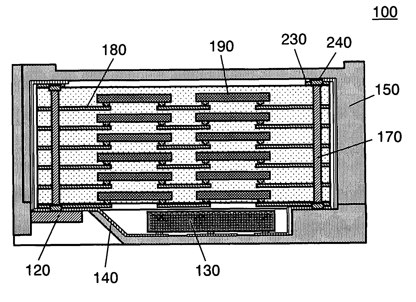
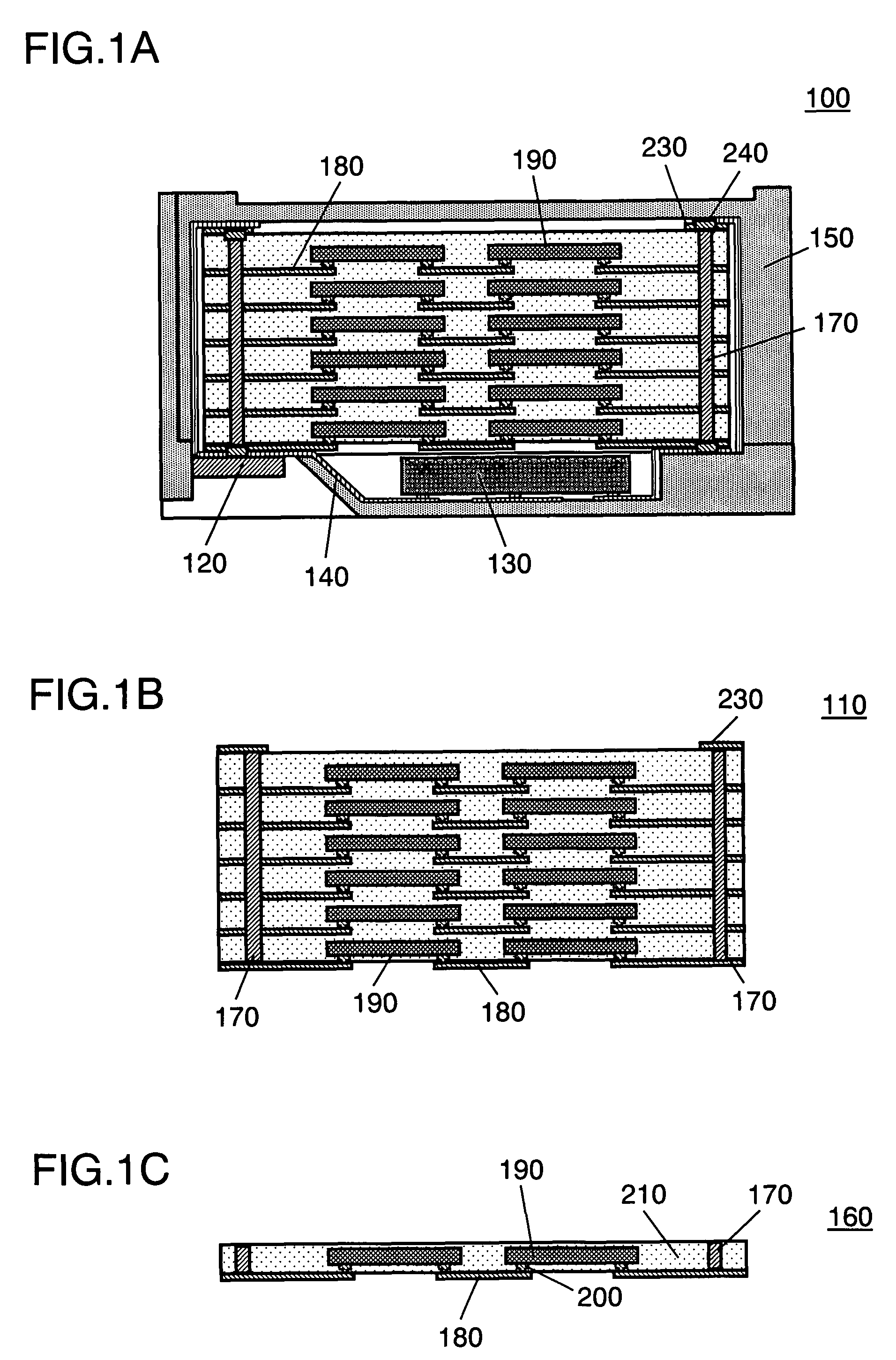
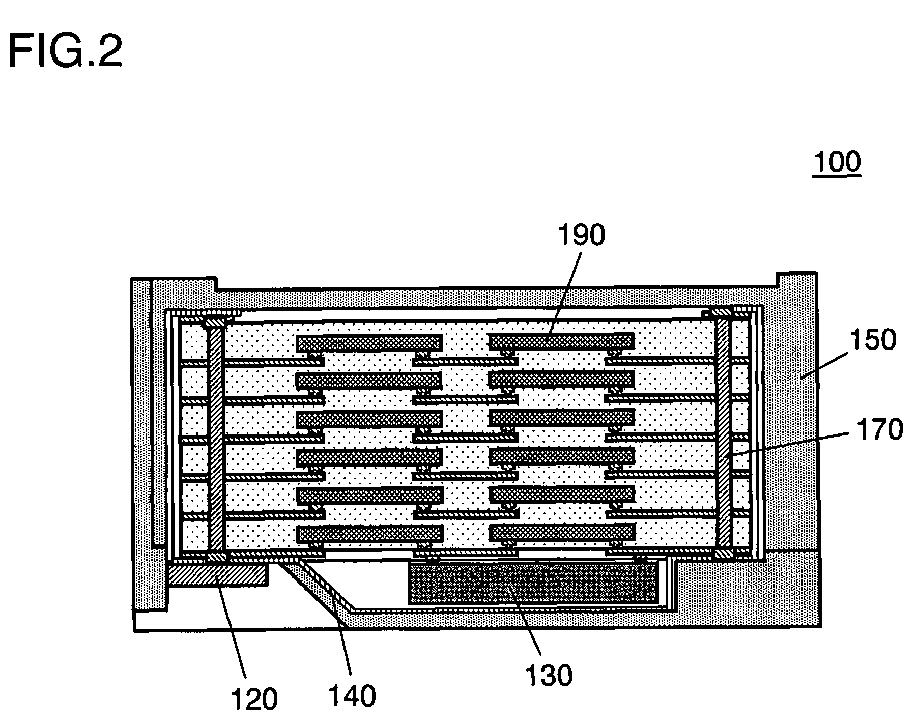
[0073]FIG. 1A is a sectional view of an electronic circuit device according to the first exemplary embodiment of the present invention; FIG. 1B is a sectional view of the substrate module unit; and FIG. 1C is a sectional view of a substrate module.

[0074]As shown in FIG. 1A, electronic circuit device 100 according to the first embodiment of the present invention has substrate module unit 110 inserted into housing 150 provided with control circuit 130 including connecting terminal 120 and semiconductor element, and with first wiring pattern 140. Then, first wiring pattern 140 formed on the inner surface of housing 150 is connected to second wiring pattern 180 of substrate module unit 110 electrically and mechanically through conductor 170 with conductive paste, solder, anisotropic conductive resin, or the like, to form electronic circuit device 100.

[0075]Here, control circuit 130, an LSI composed of semiconductor elements, is mounted on an electrode pad (not illustrated) of first wiri...

second exemplary embodiment

[0106]FIG. 5A is a sectional view of an electronic circuit device according to the second exemplary embodiment of the present invention; FIG. 5B is a sectional view of a substrate module unit; FIG. 5C is a sectional view of a substrate module. In FIGS. 5A through 5C, a component with the same makeup as that in FIG. 1 is given the same reference mark to omit its description.

[0107]In electronic circuit device 100 according to the second embodiment of the present invention, as shown in FIG. 5A, substrate module unit 250 is inserted into housing 150 including connecting terminal 120, control circuit 130, and first wiring pattern 140. Then, first wiring pattern 140 formed on the inner surface of housing 150 is connected to second wiring pattern 180 of substrate module unit 250 electrically and mechanically through conductor 170 with conductive paste or the like.

[0108]Substrate module unit 250, as shown in FIG. 5B, is structured with substrate modules 260 shown in FIG. 5C stacked in four ...

third exemplary embodiment

[0135]FIG. 10A is a sectional view of an electronic circuit device according to the third embodiment of the present invention; FIG. 10B is a sectional view of the substrate module unit; FIG. 10C is a sectional view of a substrate module. In FIGS. 10A through 10C, a component with the same makeup as that in FIG. 5 is given the same reference mark to omit its description.

[0136]In electronic circuit device 100 according to the third embodiment of the present invention, as shown in FIGS. 10A through 10C, substrate module unit 310 is inserted into housing 150 including connecting terminal 120, control circuit 130, and first wiring pattern 140. Then, first wiring pattern 140 formed on the inner surface of housing 150 is connected to second wiring pattern 180 of substrate module unit 310 electrically and mechanically through conductor 170 with conductive paste or the like.

[0137]Substrate module unit 310, as shown in FIG. 10B, is structured with substrate modules 320 shown in FIG. 10C stack...


PUM


Abstract

Electronic circuit device (100) is structured so that a substrate module unit that are formed by stacking substrate modules made of a first resin sheet with electronic component (190) embedded thereinto is inserted into housing (150) including connecting terminal (120), control circuit (130), and first wiring pattern (140), where the substrate modules are connected to each other electrically and mechanically. This electronic circuit device (100) dispenses with a mother substrate. Further, with slimming down of a substrate module, a substrate module unit with a large number of substrate modules stacked can be loaded in a limited packaging space, thus mounting greater storage capacity and higher functionality.

Description

[0001]This application is a U.S. national phase application of PCT International Application PCT / JP2005 / 015892, filed Aug. 31, 2005.TECHNICAL FIELD[0002]The present invention relates to a compact electronic circuit device incorporating substrate modules mounting electronic components thereon, in a housing, to an electronic device using the circuit device, and to a method for manufacturing the circuit device.BACKGROUND ART[0003]In recent years, with higher functionality of IC cards and greater storage capacity of memory cards, an electronic circuit device has been demanded that mounts semiconductor elements and other components with high density. Still, with higher functionality and reduction in the size and weight of mobile devices, an electronic circuit device requires higher functionality and compactification. For a memory card, for example, how to increase its storage capacity within its standardized size is important. For a circuit substrate, meanwhile, as well as an approach to...

Claims


Application Information

Patent Timeline
Patent Type & Authority Patents(United States)
IPC IPC(8): H01R12/16H01L25/065H01L25/07H01L25/10H01L25/11H01L25/18
CPCG11C5/04H01L25/0652H01L25/18H01L24/24H01L24/96H01L2924/15331H01L23/5387H01L23/5389H01L25/105H01L2924/01078H05K1/185H05K1/189H05K3/4614H01L2225/1035H01L2225/1058H01L24/92H01L2224/16225H01L2224/24137H01L2224/32145H01L2224/73267H01L23/5386H01L2224/24227
Inventor SAKURAI, DAISUKEONO, MASAHIRONISHIKAWA, KAZUHIRO
Owner PANASONIC CORP
Why Eureka
Try Eureka