

High performance flexible substrate thin film transistor and method
a flexible substrate, transistor technology, applied in the direction of thermoelectric device junction materials, electrical apparatus, semiconductor devices, etc., can solve the problems of low mobility of organic materials, low performance of most organic thin film transistors, and inability to produce inorganic thin film transistors compatible with flexible substrates. achieve the effect of further reducing the state of the interfa
- Summary
- Abstract
- Description
- Claims
- Application Information
AI Technical Summary
Benefits of technology
Problems solved by technology
Method used
Image

Examples
Embodiment Construction
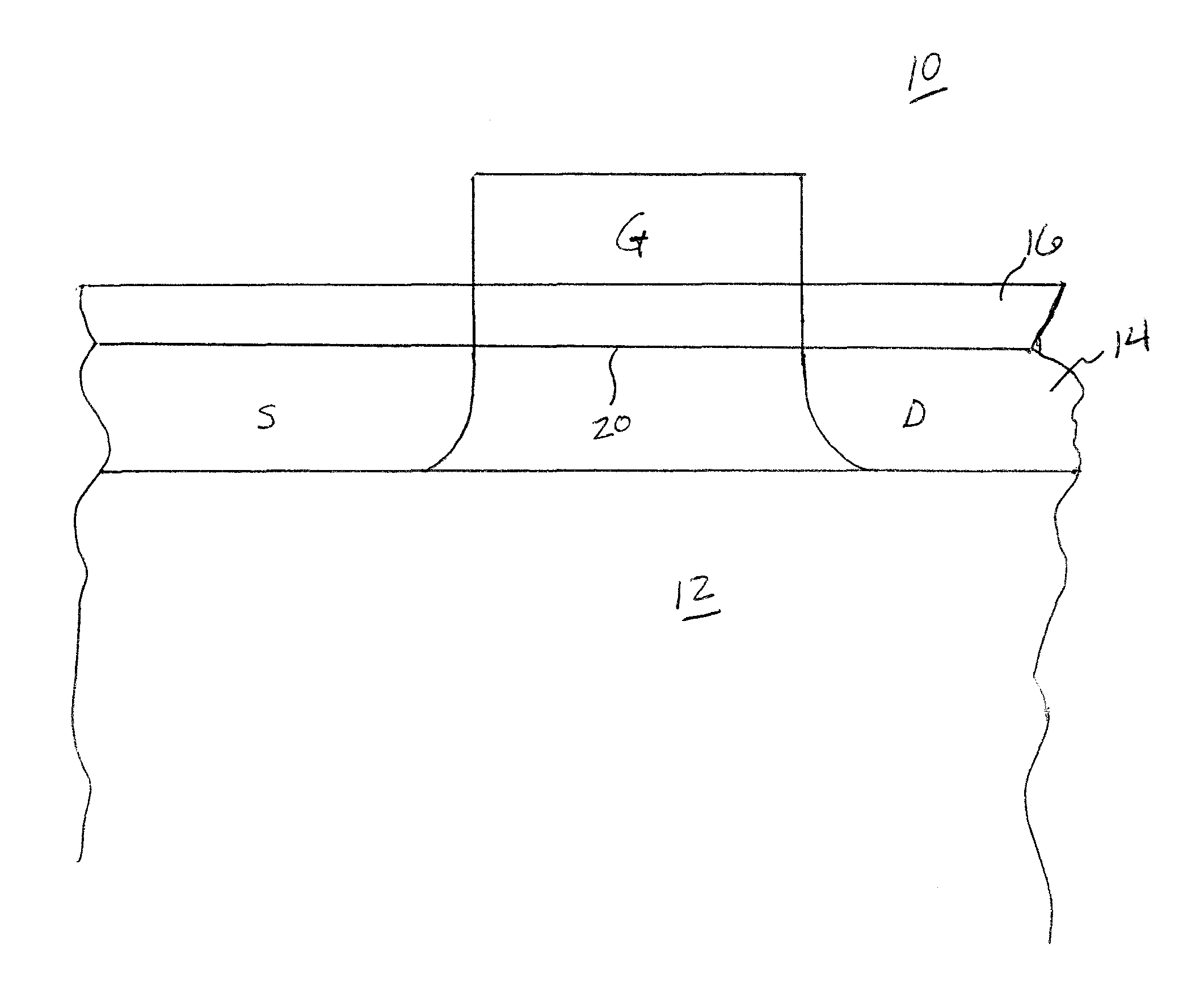
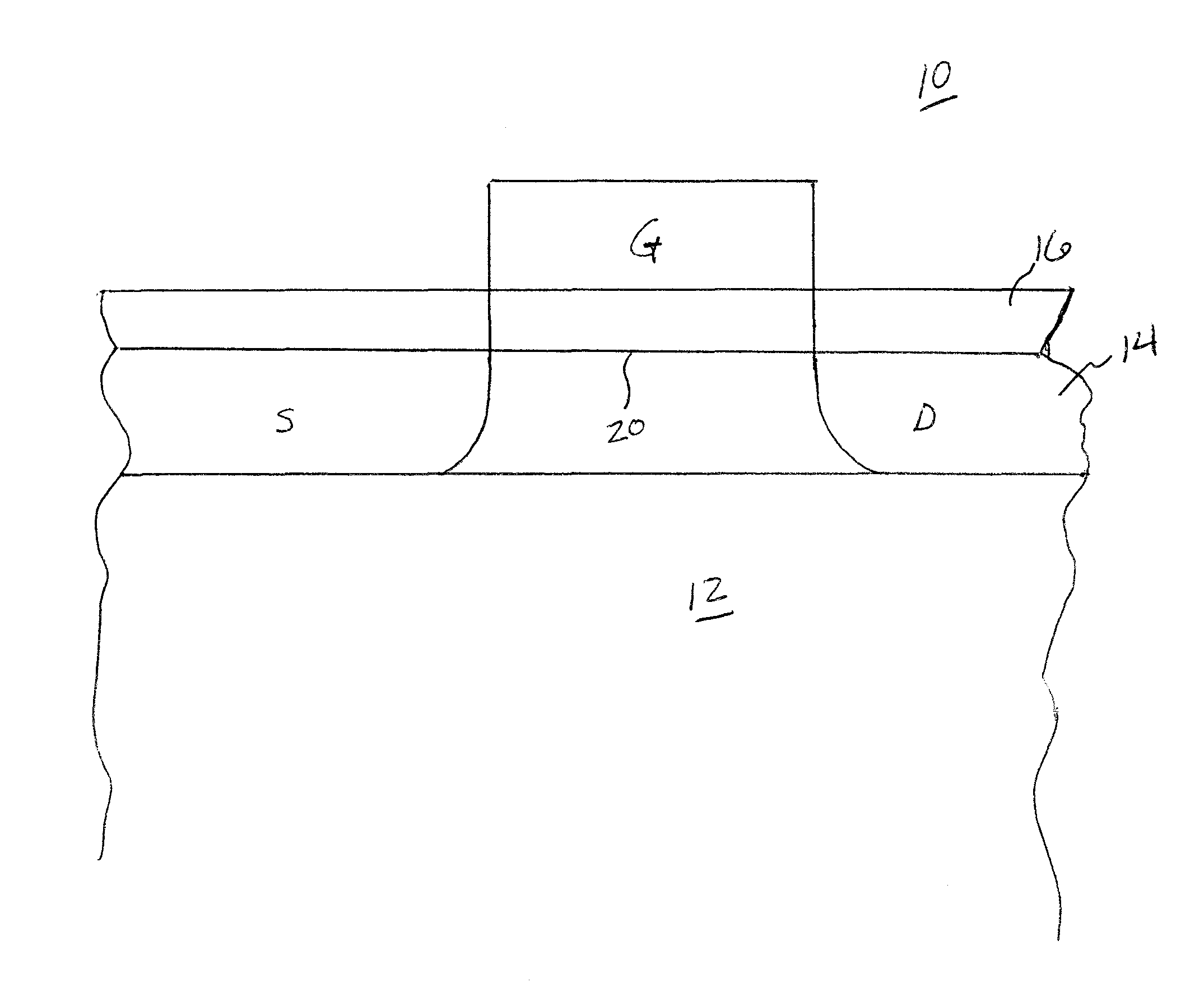
[0016]Turning now to the drawing, a thin film transistor (TFT) 10 in accordance with the present invention is illustrated. In this embodiment, TFT 10 is positioned on a substrate 12 that is a flexible substrate but may be any other convenient material. A layer 14 of semiconductor material is positioned on substrate 12. Layer 14 is formed of a metal oxide that has well known semiconductor traits the primary one of which is very high mobility for carriers (i.e. electrons or holes). Typical metal oxides that can be used as semiconductors include ZnO, InO, InZnO, and InGaZnO. Further, all of these metal oxides are transparent and can be deposited at low temperatures and in sufficiently thin layers to be relatively flexible. Metal oxide thin film transistors are attractive for device applications because of their transparency and very high mobility even when they are deposited at room temperatures.
[0017]A thin layer 16 of organic dielectric material is deposited on semiconductor layer 14...
PUM
| Property | Measurement | Unit |
|---|---|---|
| source voltage | aaaaa | aaaaa |
| temperatures | aaaaa | aaaaa |
| flexible | aaaaa | aaaaa |
Abstract
Description
Claims
Application Information