Low power scan shifting with random-like test patterns

a low-power scan and random-like test technology, applied in the field of scan chain testing, can solve the problems of excess power consumption, increased temperature beyond the normal level achieved, and inherently introduced defects in some percentage of manufactured devices of microchips, etc., and achieve the effect of reducing toggling

Inactive Publication Date: 2010-08-17
AVAGO TECH WIRELESS IP SINGAPORE PTE
View PDF4 Cites 11 Cited by
  • Summary
  • Abstract
  • Description
  • Claims
  • Application Information

AI Technical Summary

Benefits of technology

[0016]Accordingly, an aspect of the present invention is a method to minimize the toggling during shifting in and shifting out of test patterns in a scan chain, by filling the “don't cares” of a test set with values that appear random within a single test pattern.
[0021]Hence the present invention is a process to reduce the toggling during shifting in and shifting out of test patterns while maintaining random-like filling of don't cares. Since the amount of toggling is proportional to the power consumption during shifting, less toggling translates to less power consumption. Finally, the random filling of don't cares, as opposed to 0-fill, 1-fill, or adjacent fill, increases defect detection.
[0022]The sum total of all of the above advantages, as well as the numerous other advantages disclosed and inherent from the invention described herein, creates an improvement over prior techniques.

Problems solved by technology

Fabrication of microchips inherently introduces defects into some percentage of manufactured devices, which necessitates a thorough test of the chips to ensure defective devices are not shipped.
An unfortunate result of using prior art scan path architecture to test a device is excess power consumption and often increased temperature beyond normal levels achieved during functional mode.
Shifting data into the scan chains causes an excessive amount of switching, or toggling, of circuit nodes, much greater than the switching level achieved during functional mode.
Excess power and temperature during test can cause good devices to fail and can reduce device reliability.
Shifting in each test pattern is a slow process due to the length of the scan chains.
To reduce test cost (tester memory requirements and test time), compaction and compression is used to reduce the total number of test patterns, but this increases the switching activity caused by each test pattern.
Furthermore, the data is shifted into the scan chains at as high a clock frequency as possible (albeit this clock frequency is much lower than the functional clock frequency due to the unoptimized scan paths).
Peak power consumption is important when power and ground lines are sized to handle peak power drawn by the device during functional mode.
If peak power consumption during test exceeds the rating of the power and ground lines, large current spikes can flow that damage the device.
If the activity levels during test exceed the levels expected during functional mode, the device can overheat and damage can occur.
However, the added logic gate or multiplexer on the functional path, called blocking logic, increases the delay of the functional path, which is undesirable.

Method used


Image

  • Low power scan shifting with random-like test patterns
  • Low power scan shifting with random-like test patterns
  • Low power scan shifting with random-like test patterns

Examples


Embodiment Construction

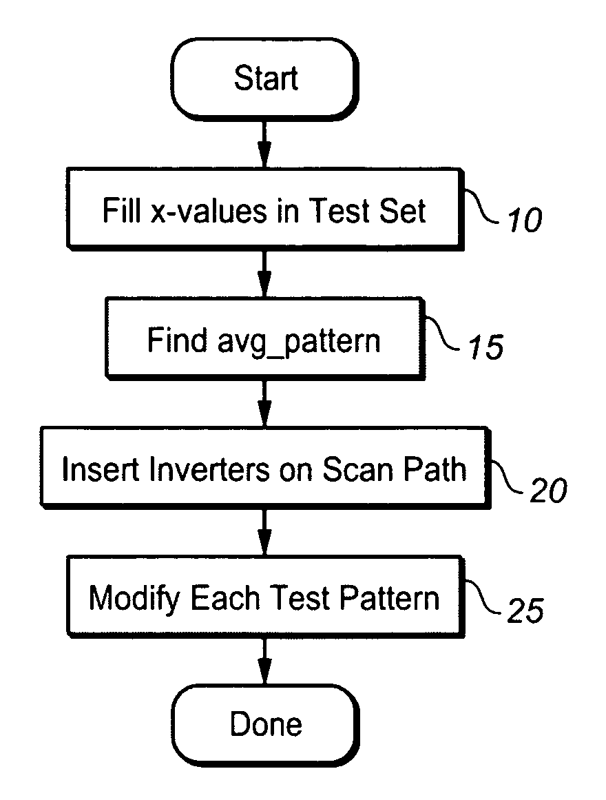
[0033]The present invention is a method to insert logic gates on the scan paths and modify the test patterns used in these scan paths accordingly, to simultaneously reduce the amount of toggling during shifting and increase the randomness of the “don't care” bits of each test pattern, and the resulting apparatus achieved by such method when constructing and designing an integrated circuit (IC) such as an ASIC, using the methodology of logical and physical design to meet all timing and power constraints. By reducing the amount of toggling during shifting, the shift power is reduced. By increasing the randomness of the “don't care” bits within a test pattern, the collateral coverage is increased and more defective chips are detected. Reducing the amount of toggling and / or increasing the collateral coverage can be termed modifying the scan path, or scan path modification, that reduces the shift power and / or increases collateral coverage over a scan path that is designed without the ben...


PUM


Abstract

An apparatus and method to design an integrated circuit (IC) to reduce the toggling during shifting in and shifting out of test patterns in a IC having scan chains, while maintaining random-like filling of the “don't cares” of a test set. An average pattern of test patterns of a test set is found for both cases of where the test set is fully specified and not fully specified, inverters are judiciously inserted into the scan path and each test pattern is then modified by XOR-ing it with the average test pattern to produce a modified test pattern, which produces less toggling, translating to less power consumption. Further, the random filling of don't cares, as opposed to 0-fill, 1-fill, or adjacent fill, increases defect detection through collateral coverage.

Description

CROSS-REFERENCE TO RELATED APPLICATIONS[0001][none]BACKGROUND OF THE INVENTION[0002]1. Field of Invention[0003]The present invention relates generally to the field of testing of semiconductor logic, in particular to scan chain testing.[0004]2. Description of Related Art[0005]Fabrication of microchips inherently introduces defects into some percentage of manufactured devices, which necessitates a thorough test of the chips to ensure defective devices are not shipped. In a scan-based design of a microchip, test data is input to the microchip when in test mode, and the output is observed and compared to a predicted output. Registers, such as flip-flops or latches, are connected in one or more scan chains, which are used to gain access to internal nodes of the microchip. Test patterns are shifted into the microchip via the scan chain(s), with clock signals pulsed to test the circuit during the “capture cycle(s).” The results of the capture cycles are then shifted out to the microchip ou...

Claims


Application Information

Patent Timeline
Patent Type & Authority Patents(United States)
IPC IPC(8): G01R31/28G06F11/00
CPCG01R31/318385G01R31/318544
Inventor CHMELAR, ERIK
Owner AVAGO TECH WIRELESS IP SINGAPORE PTE
Why Eureka
Try Eureka