Substrate treatment device and manufacturing method of semiconductor device

a technology of substrate treatment and manufacturing method, which is applied in the direction of lighting and heating apparatus, furnace types, furnaces, etc., can solve the problems of shortening the maintenance cycle, and achieve the effects of preventing by-product attachment and liquefaction, preventing any possible temperature reduction of exhaust gas, and prolonging the maintenance cycl

Active Publication Date: 2010-09-14
KOKUSA ELECTRIC CO LTD
View PDF13 Cites 9 Cited by
  • Summary
  • Abstract
  • Description
  • Claims
  • Application Information

AI Technical Summary

Benefits of technology

[0020]The invention is proposed to solve the problems described above, and an object thereof is to provide a substrate treatment device that can lengthen the maintenance cycle, and prevent any by-product from falling on substrates even if it is accumulated, and a manufacturing method of a semiconductor device.
[0021]Moreover, another object is to prevent any possible temperature reduction of an exhaust gas after a treatment, prevent by-product attachment and liquefaction of the gas after the treatment, and increase the serviceability ratio by preventing substrate pollution or by lengthening the maintenance cycle.Means for Solving the Problems

Problems solved by technology

Moreover, if a polyimide baking process is executed, the temperature is reduced when the polyimide gas vaporized as a result of baking is exhausted, thereby possibly resulting in liquefaction.
The polyimide liquefied as such becomes a cause of pollution with respect to the wafers 13, and also a cause of shortening the maintenance cycle such as removing any attached polyimide.

Method used


Image

  • Substrate treatment device and manufacturing method of semiconductor device
  • Substrate treatment device and manufacturing method of semiconductor device
  • Substrate treatment device and manufacturing method of semiconductor device

Examples


first embodiment

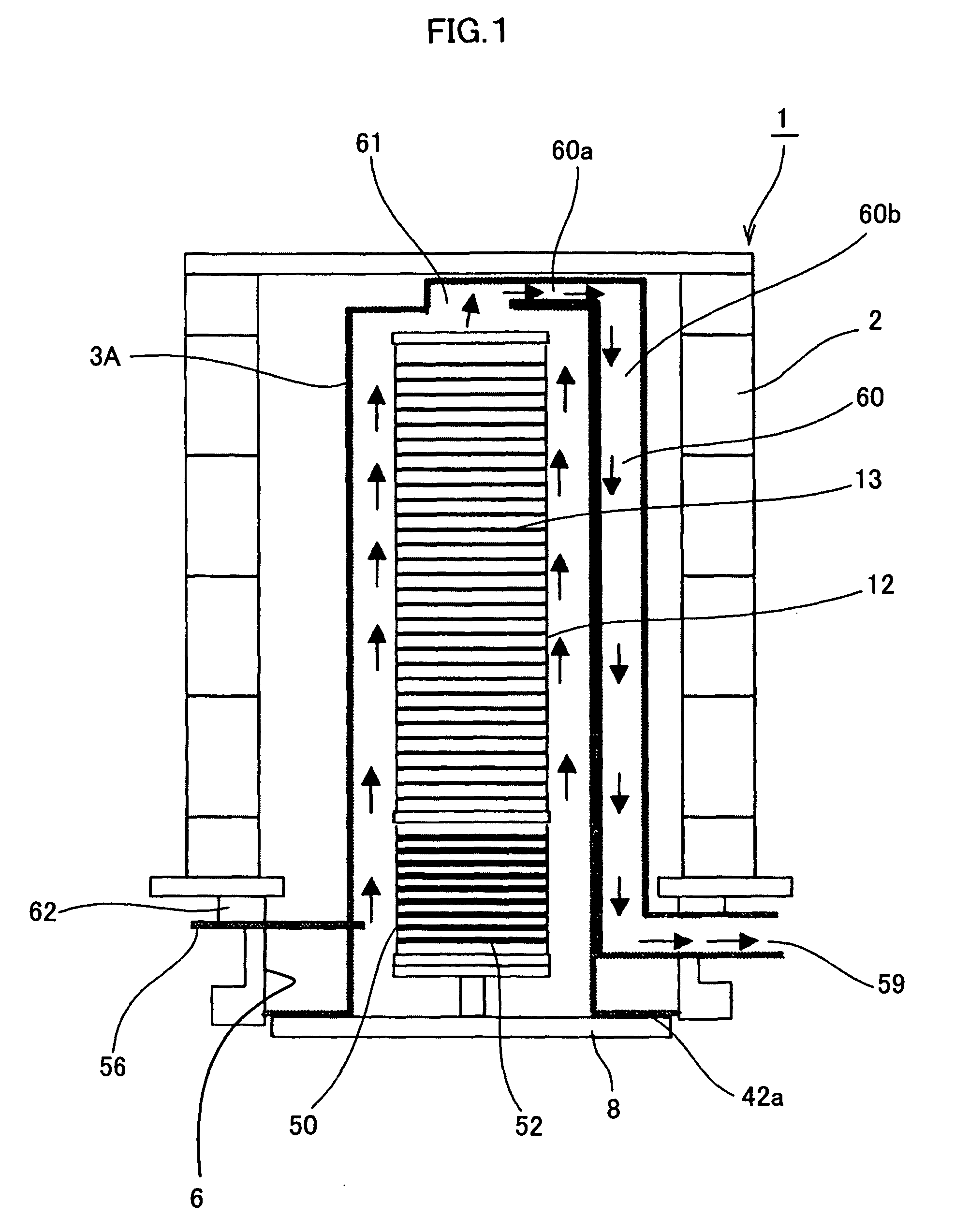
[0043]FIG. 1 is a diagram showing an exemplary treatment furnace (reaction furnace) 1 of a first embodiment of the invention.

[0044]This treatment furnace 1 carries therein a quartz-made reaction tube 3A, and the reaction tube 3A is of a cylindrical shape whose lower end portion is left open. The open lower end portion of the reaction tube 3A is shaped like a flange, and the tip end of a flange 42a is linked to a support base 62 for placement. The area around the reaction tube 3A not including the support base 62 is provided with the heater 2.

[0045]The furnace port section being the area left open below the reaction tube 3A is so configured as to be sealed air tight when the sealing cap 8 comes in contact with the lower surface of the flange 42a via an O ring that is not shown. The sealing cap 8 is supporting the boat 12, and is able to move up and down together with the boat 12. Between the sealing cap 8 and the boat 12, a heat insulation plate support member 50 is provided.

[0046]Th...

second embodiment

[0078]Described next is a second embodiment. FIG. 4 shows an exemplary treatment furnace for use in a substrate treatment device of the second embodiment.

[0079]The heater (referred also to as heating device) 2 is provided upright on a heater base 17. The heater 2 is provided with a heat generator 18 on the inner wall surface, and the heat generator 18 is divided into any predetermined number of zones in the vertical direction. The zones being the division results are each provided individually so that heating is controlled.

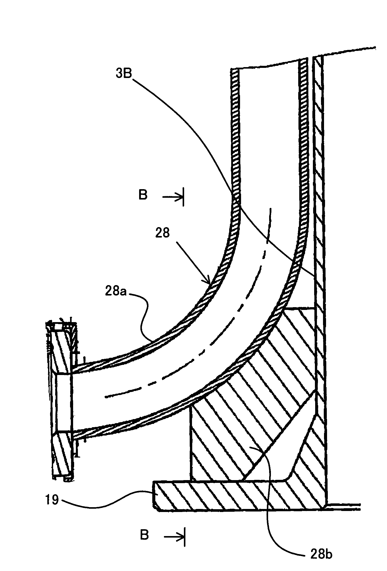
[0080]A reaction tube 3B is provided upright on an inlet flange 19 that is supported by the heater base 17 or the upper surface of a spare chamber (not shown) provided at the lower portion, and between the reaction tube 3B and the above-described inlet flange 19, a sealing member is sandwiched to be air tight. The aperture at the lower end of the above-described inlet flange 19 forms the furnace port section 7, and the furnace port section 7 is closed to be air ti...

third embodiment

[0139]FIG. 11 shows a treatment furnace of a substrate treatment device of a third embodiment.

[0140]In the configurations of the first and second embodiments, especially when a heat treatment is applied to a plurality of wafers that are each coated with an organic material or are not yet completely free from any organic material thereon, the gas including the material coated on the wafers or the gas including the by-product generated from the remaining is moved backward and diffused to the upstream side from the wafers in the furnace so that the gas is attached inside of the treatment chamber. FIG. 12 shows such a state.

[0141]If this is the case, when the temperature on the side walls in the treatment chamber is equal to or higher than 200° C., the gas will become like a film (layer), and thus it will not easily peeled off or scattered. However, at any portion of the side walls (low-temperature portion at the furnace port) LTP with the temperature lower than 200° C., it will be easi...


PUM

PropertyMeasurementUnit
temperatureaaaaaaaaaa

Abstract

An object of the invention is to provide a substrate treatment device that can lengthen the maintenance cycle, and prevent any by-product from falling on substrates even if it is accumulated, and a manufacturing method of such a substrate treatment device, and an embodiment of the invention is directed, comprising: a treatment chamber that subjects a substrate to a treatment while keeping hold of it by a substrate retention member; a reaction tube that configures the treatment chamber; a heating device that is disposed around the reaction tube for heating the treatment chamber; and an exhaust tube that is linked to the reaction tube on an upper side than the substrate inside of the treatment chamber and is extended downward from the heating device, and exhausts a gas inside of the reaction tube in which an extension portion as a result of the extension is disposed away from the reaction tube.

Description

TECHNICAL FIELD[0001]The present invention relates to a substrate treatment device for subjecting a substrate to a heat treatment and a manufacturing method of a semiconductor device and, more specifically, to a substrate treatment device that manufactures a semiconductor device by subjecting a substrate such as silicon wafer and glass substrate to a substrate treatment including thin-film formation, impurity diffusion, annealing treatment, and etching, and a manufacturing method of the semiconductor device.BACKGROUND ART[0002]A substrate treatment device includes a sheet-fed substrate treatment device that performs a substrate treatment one by one, and a batch-fed substrate treatment device that performs a substrate treatment by the unit of a predetermined number of sheets. As one of the batch-fed substrate treatment device, there is a portrait-oriented substrate treatment device including a portrait-oriented treatment furnace.[0003]FIG. 19 shows a treatment furnace 1 of a portrait...

Claims


Application Information

Patent Timeline
Patent Type & Authority Patents(United States)
IPC IPC(8): H01L21/31
CPCC23C16/4412C23C16/54H01L21/67109
Inventor TERASAKI, MASATOMORITA, SHINYAIZUMI, MANABU
Owner KOKUSA ELECTRIC CO LTD
Why Eureka
Try Eureka