Power semiconductor device and method of manufacturing a power semiconductor device

a technology of power semiconductor and semiconductor device, which is applied in the direction of semiconductor device, basic electric element, electrical apparatus, etc., can solve the problems of maintaining or improving the breakdown voltage, and the conflict between reducing the on-state resistan

Active Publication Date: 2010-09-21
NXP USA INC
View PDF14 Cites 1 Cited by
  • Summary
  • Abstract
  • Description
  • Claims
  • Application Information

AI Technical Summary

Problems solved by technology

In spite of the various design features adopted, a problem that increases with increasing the cell or channel density is maintaining or improving the breakdown voltage.
The different configurations referred to above address the issue of breakdown voltage but there remains a conflict between reducing on-state resistance, especially by increasing the channel density, and improving breakdown voltage.

Method used


Image

  • Power semiconductor device and method of manufacturing a power semiconductor device
  • Power semiconductor device and method of manufacturing a power semiconductor device
  • Power semiconductor device and method of manufacturing a power semiconductor device

Examples


Embodiment Construction

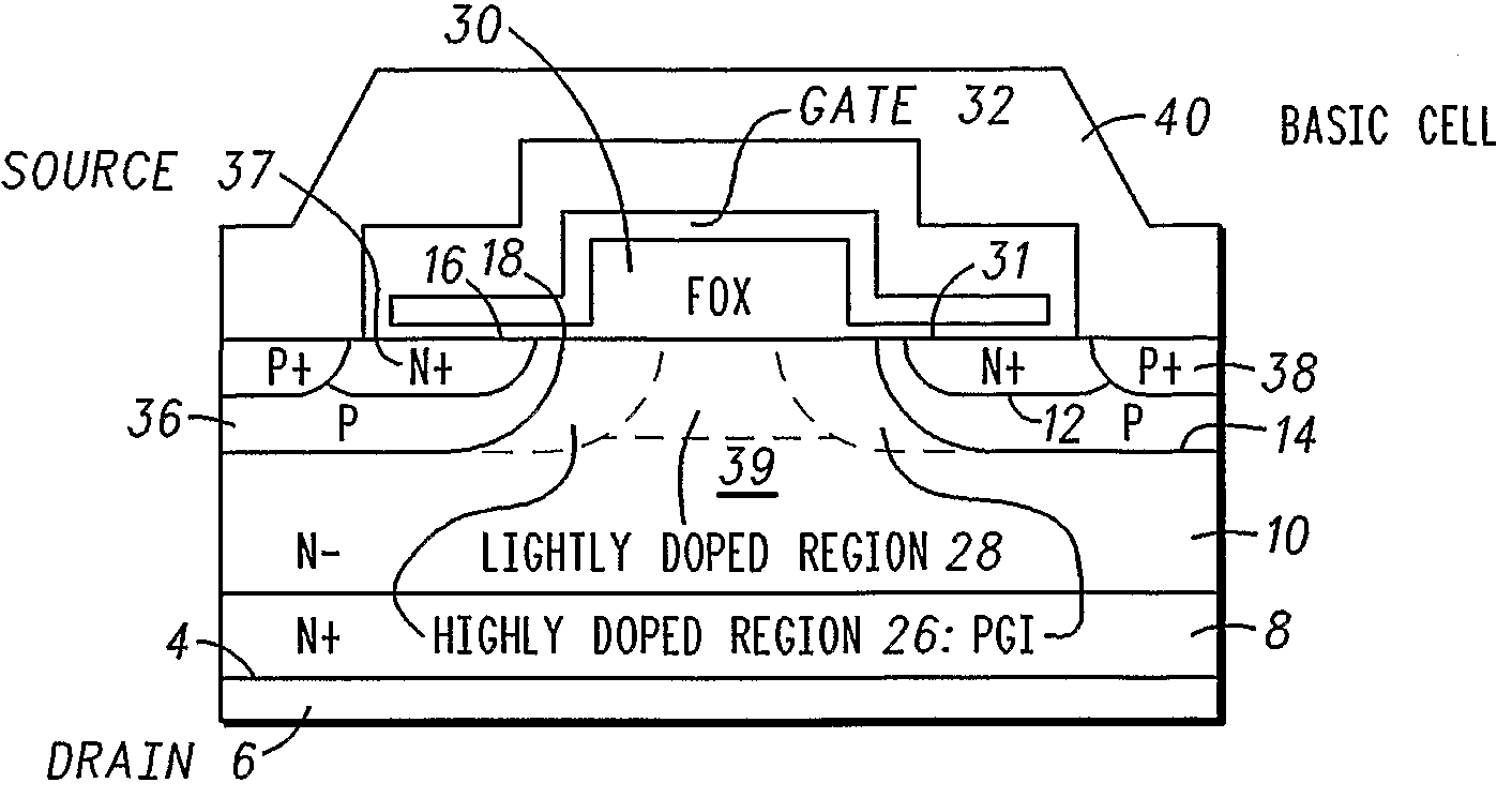
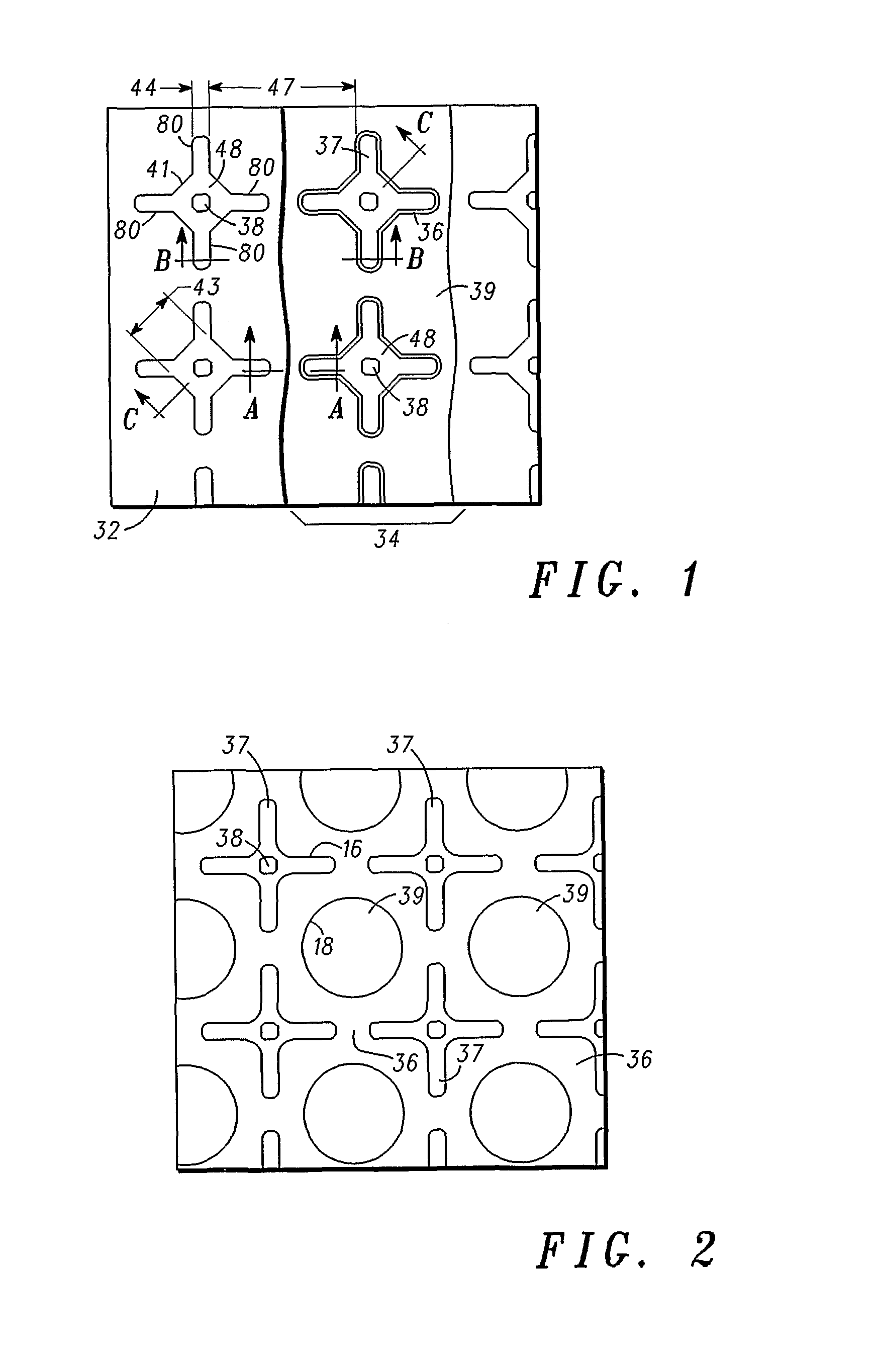
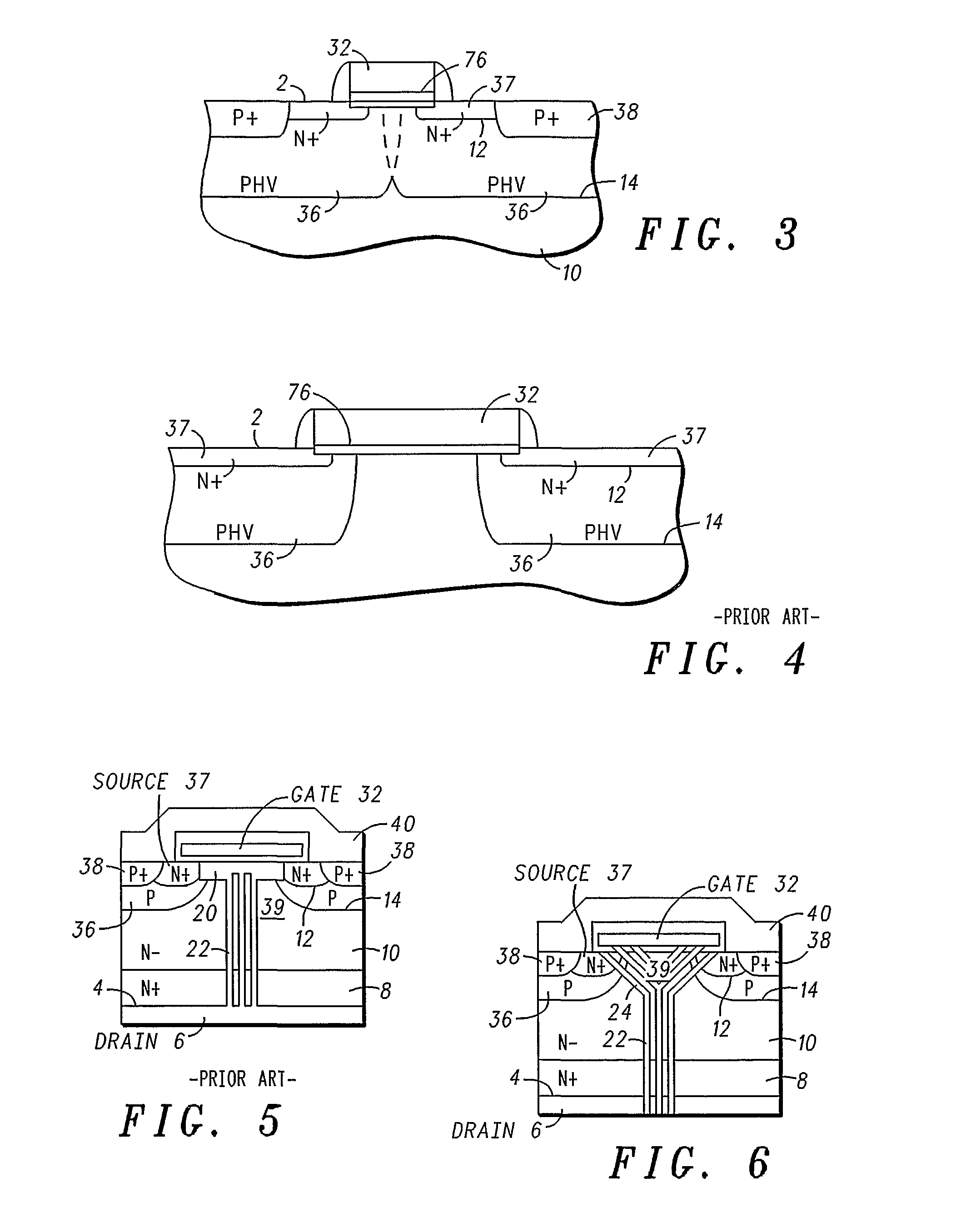
[0017]The semiconductor device shown in FIGS. 1 to 6 is a vertical insulated gate field-effect power transistor semiconductor device. The configuration of the device comprises an array of cells (only part of which is shown in the drawings) formed in a die of semiconductor material presenting a first face 2 and a second face 4 opposite to the first face. A drain electrode 6 is disposed on the second face 4 and contacts a first drain layer 8 of a first conductivity type that extends from the second face 4. A second superposed drain layer 10 also of the first conductivity type but having a lower dopant density than the first drain layer 8 extends from the first drain layer to the first face 2. Each of the basic cells comprises a source region 37 of the first conductivity type extending from the first face 2 and a base region 36 of the opposite conductivity type surrounding the source region at and below the first face. The base region 36 forms with the source and drain regions 37 and 3...


PUM


Abstract

A semiconductor power switch having an array of basic cells in which peripheral regions in the active drain region extend beside the perimeter of the base-drain junction, the peripheral regions being of higher dopant density than the rest of the second drain layer. Intermediate regions in the centre of the active drain region are provided of lighter dopant density than the rest of the second drain layer. This provides an improved compromise between the on-state resistance and the breakdown voltage by enlarging the current conduction path at in its active drain region. On the outer side of each edge cell of the array, the gate electrode extends over and beyond at least part of the perimeters of the base-source junction and the base-drain junction towards the adjacent edge of the die. Moreover, on the outer side of each edge cell, the second drain layer includes a region of reduced dopant density that extends beyond the gate electrode right to the adjacent edge of the die.

Description

FIELD OF THE INVENTION[0001]This invention relates to a power semiconductor device, especially a Metal Oxide Semiconductor Field Effect Transistor (‘MOSFET’), and a method of manufacturing such a power semiconductor device.BACKGROUND OF THE INVENTION[0002]Semiconductor devices such as MOSFETs have been used in power electronics applications due to their appreciable off-state voltage blocking capability and on-state current carrying capacity with low on-state resistance RDSON. In terms of industrial applications, power MOSFET devices are commonly used in many electronics fields such as portable electronics, power supplies and telecommunications and more particularly in many industrial applications relating to automotive electronics.[0003]Conventionally, an insulated gate FET (IGFET) configuration for a power MOSFET has a four-layer structure of alternating p-type and n-type doping superposed vertically in the body of the semiconductor die, that is to say superposed in a direction per...

Claims


Application Information

Patent Timeline
Patent Type & Authority Patents(United States)
IPC IPC(8): H01L29/74H01L21/8238
CPCH01L29/66712H01L29/7802H01L29/7811H01L29/0878H01L29/42368
Inventor REYNES, JEAN-MICHELALVES, STEPHANEDERAM, ALAINLOPES, BLANDINOMARGHERITTA, JOEL
Owner NXP USA INC
Why Eureka
Try Eureka