Photoelectric conversion device and method of producing the same, and method of producing line image sensor IC

a conversion device and photoelectric technology, applied in the direction of radiation controlled devices, semiconductor devices, semiconductor/solid-state device details, etc., can solve the problems of uneven surface of protective film with short pitch size, large variation in electric signal values, and actually a very difficult operation

Inactive Publication Date: 2010-10-19
ABLIC INC
View PDF7 Cites 2 Cited by
  • Summary
  • Abstract
  • Description
  • Claims
  • Application Information

AI Technical Summary

Benefits of technology

[0052]The object of the present invention is to provide, based on the finding that there is a causal relationship between the change in thickness of the protective film and the arrangement of a conductive material described with reference to FIG. 10, a photoelectric conversion device, a method of producing the same, and a method of producing a line image sensor IC in which the thickness of a protective film formed on the line image sensor IC is uniform, whereby the values of electric signals sent from the photoelectric conversion elements placed in each line image sensor IC can be uniform.
[0086]As a result the thickness of the protective film on the line image sensor IC is uniformized, so the reflection and interference conditions by the protective film become equal in any portion in the longitudinal direction, whereby the variation in values of electric signals sent from a plurality of photoelectric conversion elements provided in the line image sensor ICs can be suppressed.

Problems solved by technology

Forming unevenness with a short pitch size on the surface of the protective film as in the method shown in Japanese Patent Application Laid-open No. 06-260625 is actually a very difficult operation.
Further, there is a fear that the variation in the values of electric signals becomes larger depending upon the size and shape of unevenness.
Further, according to the technique of removing a portion of the protective film positioned above the light-receiving surface of the photoelectric conversion element, the protective film for protecting the photoelectric conversion element is removed, so the protection of the photoelectric conversion element becomes insufficient.
A further basic problem lies in that the cause and mechanism of variation in thickness of the protective film 4 are not accurately clarified.

Method used


Image

  • Photoelectric conversion device and method of producing the same, and method of producing line image sensor IC
  • Photoelectric conversion device and method of producing the same, and method of producing line image sensor IC
  • Photoelectric conversion device and method of producing the same, and method of producing line image sensor IC

Examples


embodiment 1

Preferred Embodiment 1

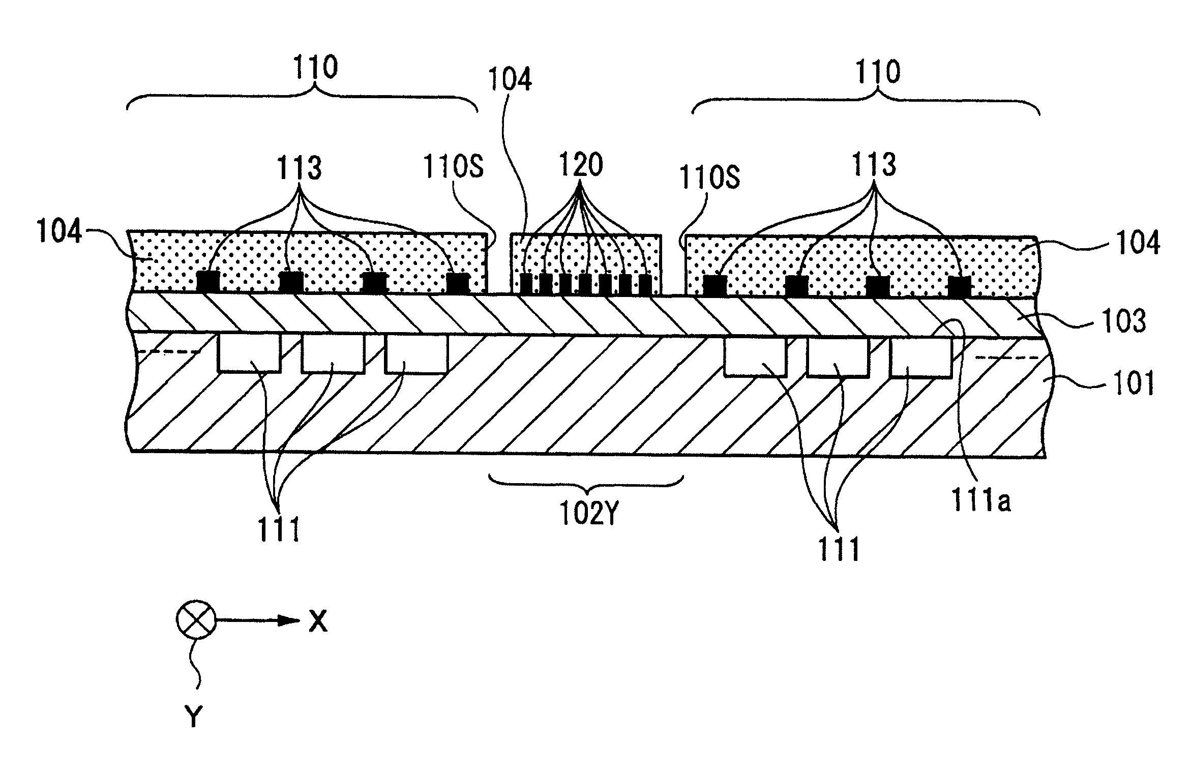
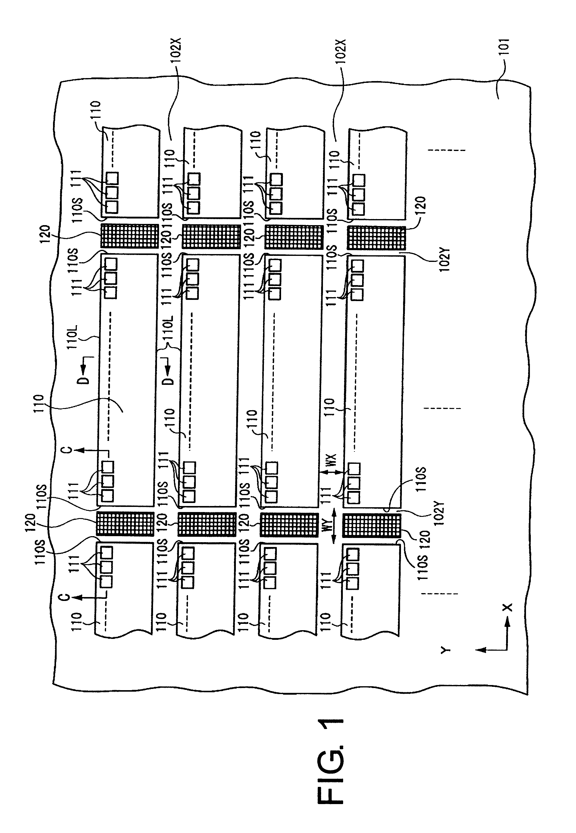
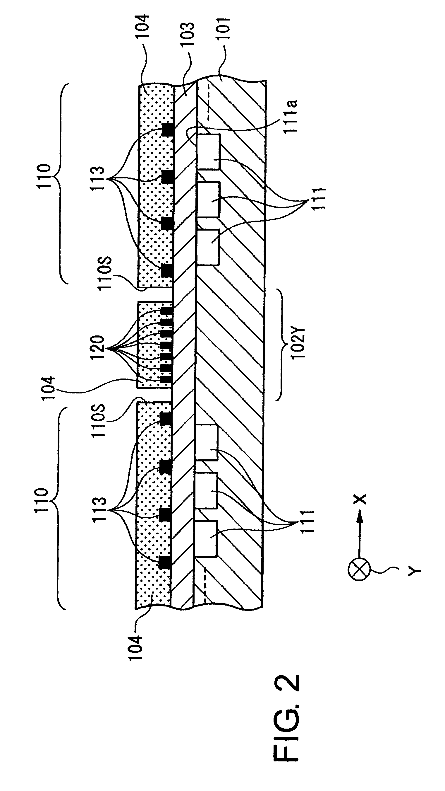
[0105]A photoelectric conversion device according to Embodiment 1 of the present invention, i.e., a photoelectric conversion device in which a plurality of line image sensor ICs are formed on a semiconductor substrate (semiconductor wafer) will be described with reference to FIG. 1, FIG. 2 showing a cross-section taken along a line C-C in FIG. 1, and FIG. 3 showing a cross-section taken along a line D-D in FIG. 1. In FIGS. 1 to 3, each member is not drawn to scale for ease of understanding of the configuration

[0106]As shown in FIGS. 1 to 3, a plurality of line image sensor ICs 110 are formed on the surface of a semiconductor substrate (semiconductor wafer) 101 in the photoelectric conversion device. For example, in the case where a wafer diameter of the semiconductor substrate 101 is 6 inches, thousands of line image sensor ICs 110 are formed on one semiconductor substrate 101.

[0107]In each line image sensor IC 110 having an elongated rectangular shape, a plura...

embodiment 2

Preferred Embodiment 2

[0147]There is also a line image sensor IC in which light-shielding aluminum (second conductive material) is provided above the electric interconnects 112 and the inter-pixel light shielding aluminum 113 (that is, the first conductive material), and the electric interconnects 112, the inter-pixel light shielding aluminum 113, and the light-shielding aluminum are buried with the protective film 104.

[0148]The light-shielding aluminum is formed substantially over the entire region of the line image sensor IC, and only a part that is placed above the light-receiving surface 111a of the photoelectric conversion device 111 is opened.

[0149]In a photoelectric conversion device having a line image sensor IC that includes not only the first conductive material but also the second conductive material, the dummy interconnects 120 as shown in Embodiment 1 are formed, whereby the thickness of the protective film 104 formed in the line image sensor IC can be uniformized.

embodiment 3

Preferred Embodiment 3

[0150]Next, a method of producing a photoelectric conversion device and a method of producing a line image sensor IC according to Embodiment 3 of the present invention will be described with reference to FIGS. 5A to 5F.

[0151]According to the production method of Embodiment 3, the photoelectric conversion device of Embodiment 1 can be produced.

[0152]First, as shown in FIG. 5A, a semiconductor substrate (P-type silicon substrate) 101 is prepared.

[0153]Next, as shown in FIG. 5B, a local oxidation of silicon (LOCOS) oxide film 103a, which is an element separation film, is formed on the surface of the semiconductor substrate 101. N-type regions constituting N-wells, P-wells, and photoelectric conversion elements (pixels) 111 of a CMOS transistor forming a signal processing circuit are formed by ion implantation. The photoelectric conversion elements 111 function as light-receiving portions of the line image sensor IC.

[0154]Next, a gate oxide film is formed, polysili...


PUM


Abstract

A plurality of line image sensor ICs 110 are formed to be arranged in X, Y directions with gaps therebetween on a semiconductor substrate 101. The gaps between the line image sensor ICs 110 become scribe lines 102X, 102Y. A pattern of dummy interconnects 120 is formed in a region where a short side 110S of an arbitrary line image sensor IC 110 is opposed to a short side 110S of another line image sensor IC 110 adjacent to the arbitrary line image sensor IC 110 in the X direction in a region where the scribe line 102Y is formed. When a material gas is generated by plasma CVD, the material gas is uniformly deposited not only on the line image sensor ICs 110, but also on the dummy interconnects 120. Consequently, a protective film with a uniform thickness can be formed on the line image sensor ICs 110.

Description

[0001]This application claims priority under 35 U.S.C. §119 to Japanese Patent Application No. JP2006-348989 filed Dec. 26, 2006, the entire content of which is hereby incorporated by reference.FIELD OF THE INVENTION[0002]The present invention relates to a photoelectric conversion device and a method of producing the same, and a method of producing a line image sensor IC, in which reduction of variation in electric signal values sent from respective photoelectric conversion elements placed in a line image sensor IC is performed.DESCRIPTION OF THE RELATED ART[0003]An image reader such as an image scanner and a facsimile includes a line image sensor IC in a reading portion in order to read an image.[0004]The line image sensor IC has an elongated rectangular shape. In such a line image sensor IC, a plurality of (e.g., 400) photoelectric conversion elements (light-receiving elements, pixels) are placed so as to be aligned in a row in a longitudinal direction, and electric interconnects ...

Claims


Application Information

Patent Timeline
Patent Type & Authority Patents(United States)
IPC IPC(8): H01L23/544
CPCH01L27/14632H01L27/14636
Inventor OMI, TOSHIHIKOMIMURO, YOICHI
Owner ABLIC INC
Why Eureka
Try Eureka