Adaptive current sense amplifier with direct array access capability

a current sense amplifier and adaptive technology, applied in the direction of amplifiers with semiconductor devices/discharge tubes, dc-amplifiers with dc-coupled stages, etc., can solve the problems of impracticality of pmos devices, large substrate area, icell and ir

Active Publication Date: 2010-10-26
LONGITUDE FLASH MEMORY SOLUTIONS LTD
View PDF76 Cites 14 Cited by
  • Summary
  • Abstract
  • Description
  • Claims
  • Application Information

AI Technical Summary

Problems solved by technology

A drawback to an arrangement like that of FIG. 6 can be that the use of resistors within a load circuit 606, whether implemented as polycrystalline (polysilicon) resistors or substrate diffusion regions, can require considerable substrate area in the event currents Icell and Iref are small.
At the same time, precharging data nodes (602 and 604) to a value VCC−Vtp using diode connected PMOS devices can be impractical at low voltage applications as such a Vtp drop from VCC can create “headroom” issues for the sense amplifier and for the memory cell.
That is, the working range of voltages for sensing operations can be undesirable small.
Yet another problem that can arise from a conventional approach like that of FIG. 6 can be that some nonvolatile memory technologies have cell current values that can change with temperature and / or due to aging of the memory cells.

Method used


Image

  • Adaptive current sense amplifier with direct array access capability
  • Adaptive current sense amplifier with direct array access capability
  • Adaptive current sense amplifier with direct array access capability

Examples


first embodiment

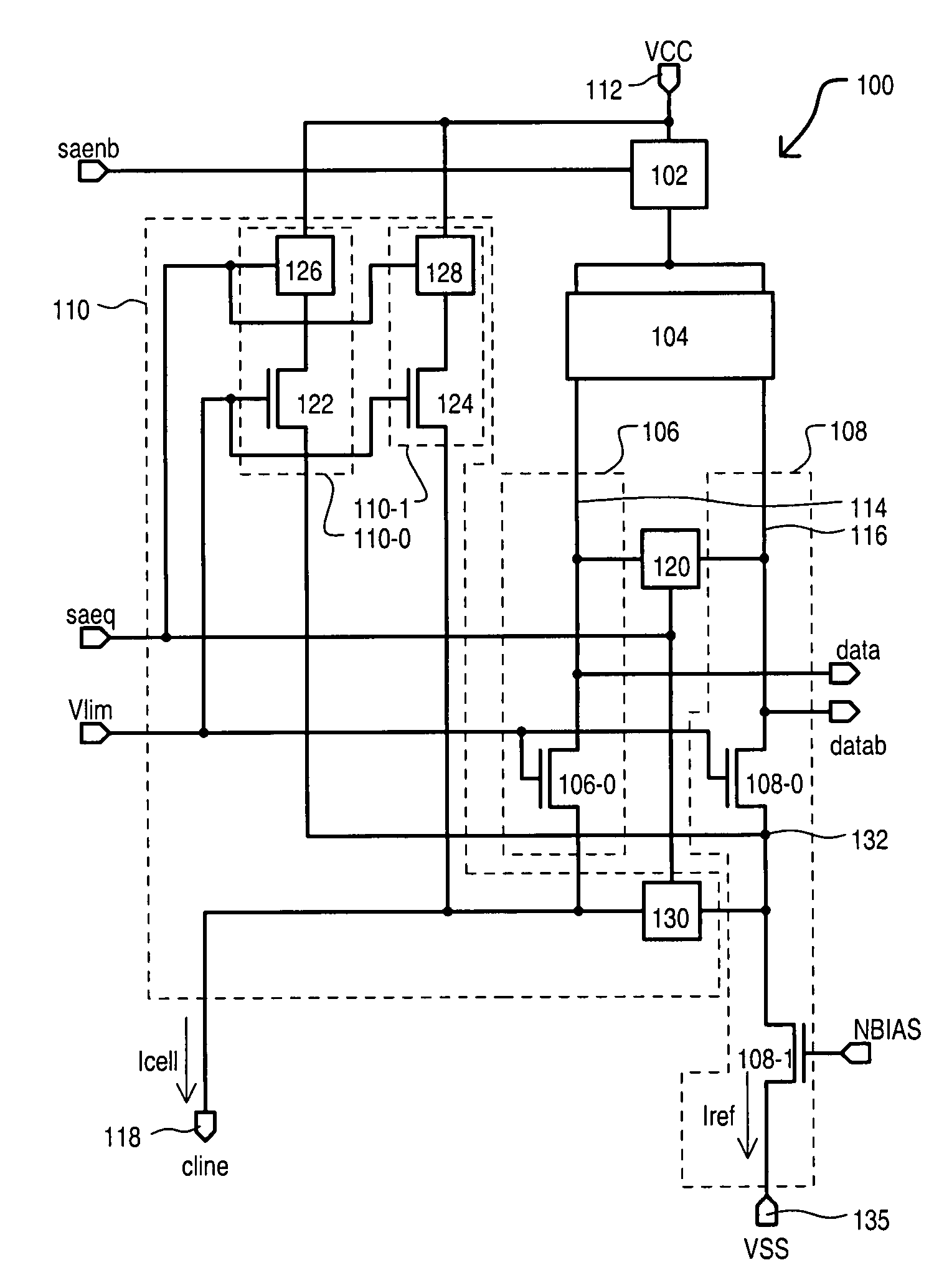
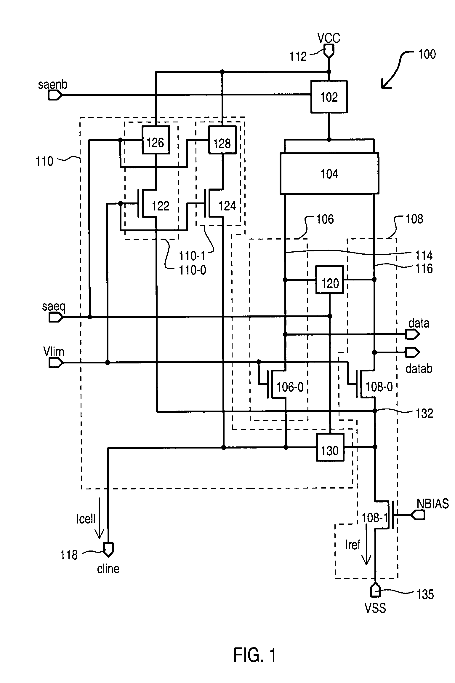
[0025]Referring now to FIG. 1, a sense amplifier (SA) circuit is shown in a block schematic diagram and designated by the general reference character 100. A SA circuit 100 can include an enable section 102, a load circuit 104, a data current leg 106, a reference current leg 108, and a precharge circuit 110.

[0026]An enable section 102 can be controlled by a sense amplifier enable signal saenb. In a precharge mode, enable section 102 can be disabled and provide a high impedance path. In sense mode, enable section 102 can be enabled, coupling load circuit 104 to high power supply node 112. A load circuit 104 can provide essentially the same impedance to both a data current leg 106 and a reference current leg 108.

[0027]A data value can be sensed according to a differential voltage generated between first data node 114 of data current leg 106, and a second data node 116 of reference current leg 108. Such a differential voltage can be generated according to a difference between a data cu...

second embodiment

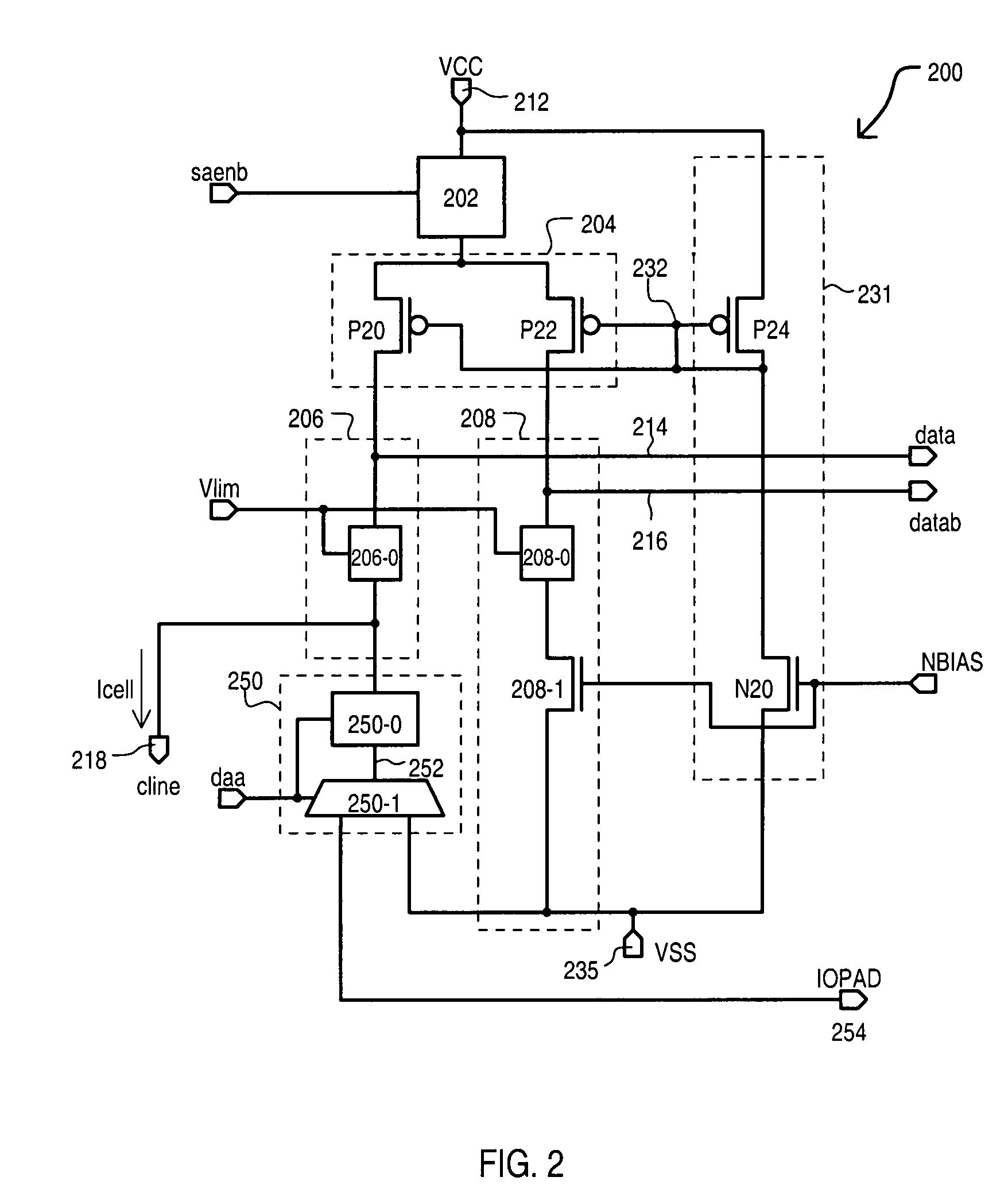
[0041]Referring now to FIG. 2, a sense amplifier circuit is shown in a block schematic diagram and designated by the general reference character 200. A sense amplifier circuit 200 can include some of the same general sections as FIG. 1, accordingly, like sections are referred to by the same reference character but with the first digit being a “2” instead of a “1”.

[0042]Unlike the embodiment of FIG. 1, sense amplifier circuit 200 shows an adaptive bias circuit 231 and direct access circuit 250. In the arrangement of FIG. 2, a load circuit 204 can be an active load circuit controlled according to a potential at a load control node 232. In the particular example shown, load circuit 204 can include first load transistor P20 coupled between enable circuit 202 and data current path 206, and a second load transistor P22 coupled between enable circuit 202 and reference current path 208. Transistors P20 and P22 can have gates commonly connected to load control node 232.

[0043]An adaptive bia...

third embodiment

[0049]Referring now to FIG. 3, a sense amplifier circuit 300 is shown in a block schematic diagram. A sense amplifier 300 can include some of the same general sections as FIGS. 1 and 2, accordingly, like sections are referred to by the same reference character but with the first digit being a “3” instead of a or “2”.

[0050]Unlike the previous embodiments, sense amplifier 300 shows an arrangement in which an enable circuit 302 can include a p-channel IGFET having a source-drain path connected between a high power supply node 312 and a load circuit 304. Similarly, enable circuits (326 and 328) within precharge circuit 310 can be p-channel IGFETs, with gates coupled to receive the inverse of the equalization signal saeq via an inverter 130.

[0051]Equalization circuits 320 and 330 for sense amplifier 300 can be formed with complementary transistors in a CMOS passgate type configuration. Accordingly, p-channel devices within such passgates can receive the inverse of signal saeq via an inv...


PUM


Abstract

A current sense amplifier can include an active load circuit having a first load device and second load device coupled in parallel to a first power supply node. A first load device and second load device can provide an impedance that varies according to a potential at a load control node. A reference current circuit can be coupled between the first load device and a second power supply node that includes a current reference section that provides an impedance according to a bias voltage. A data current circuit can be coupled between the second load device and a plurality of memory cells. An adaptive bias circuit can be coupled between the first power supply and the second power supply node and can include a bias section coupled to the load control node that provides an impedance according to the bias voltage.

Description

[0001]This application claims the benefit of U.S. Provisional Patent Application Ser. No. 60 / 854,599 filed on Oct. 24, 2006, the contents of which are incorporated by reference herein.TECHNICAL FIELD[0002]The present invention relates generally to sense amplifier circuits, and more particularly to current sense amplifier circuits that can be included in memory devices.BACKGROUND OF THE INVENTION[0003]Memory devices, such as nonvolatile memory devices, can use single ended current sensing schemes. One example of a single ended current sensing scheme is shown in FIG. 7 and designated by the general reference character 700. A single ended current sensing arrangement 700 can include a number of memory cells (e.g., 702) each connected to a bit line (BLn, BL(n+1)) and a word line (WL0 to WLm). When a memory cell (e.g., 702) is selected, it can create a current path to draw a current Icell. A memory cell current (Icell) can vary according to a data value stored. Sense amplifiers (SAn, SA(n...

Claims


Application Information

Patent Timeline
Patent Type & Authority Patents(United States)
IPC IPC(8): G11C7/02
CPCG11C7/062G11C2207/063
Inventor RAGHAVAN, VIJAY KUMAR SRINIVASA
Owner LONGITUDE FLASH MEMORY SOLUTIONS LTD
Why Eureka
Try Eureka