Manufacturing method for ink jet recording head chip, and manufacturing method for ink jet recording head

a manufacturing method and recording head technology, applied in the manufacturing of instruments, recording devices, manufacturing tools, etc., can solve the problems of difficult to reliably (accurately) mass-produce ink jet recording head chips, inferior in terms of manufacturing efficiency, and limited method disclosed in u.s. patent no. 6,107,209. achieve the effect of higher efficiency

Active Publication Date: 2010-11-02
CANON KK
View PDF23 Cites 5 Cited by
  • Summary
  • Abstract
  • Description
  • Claims
  • Application Information

AI Technical Summary

Benefits of technology

[0015]Thus, the primary object of the present invention is to provide an ink jet recording head chip manufacturing method for more reliably mass-producing ink jet recording head chips, at a higher level of accuracy than an ink jet recording head chip manufacturing method in accordance with the prior art. More specifically, the primary object of the present invention is to manufacture an ink jet recording head chip, the common ink delivery channels of which are substantially narrower than that of an ink jet recording head chip manufactured with the use of the ink jet recording head chip manufacturing method in accordance with the prior art, at a substantially higher level of precision and in a substantially shorter length of time, compared to the method in accordance with the prior art.
[0017]The present invention makes it possible to reliably mass-manufacture ink jet recording head chips, at a substantially higher level of efficiency.

Problems solved by technology

However, the method disclosed in U.S. Pat. No. 6,107,209 is limited in terms of the distance from the bottom surface of a substrate to the apex of the “”-shaped cross section of the common ink delivery channel.
Further, when this method is used, the cross-sectional shape, in which each common ink delivery channel will be finished, is affected by the oxygen concentration of the silicon substrate, making it difficult to reliably (accurately) mass-produce ink jet recording head chips.
Therefore, this method is problematic in that it is inferior in terms of manufacture efficiency, because it takes more time to make a hole in a silicon substrate by dry etching than by wet etching.

Method used


Image

  • Manufacturing method for ink jet recording head chip, and manufacturing method for ink jet recording head
  • Manufacturing method for ink jet recording head chip, and manufacturing method for ink jet recording head
  • Manufacturing method for ink jet recording head chip, and manufacturing method for ink jet recording head

Examples


embodiment 1

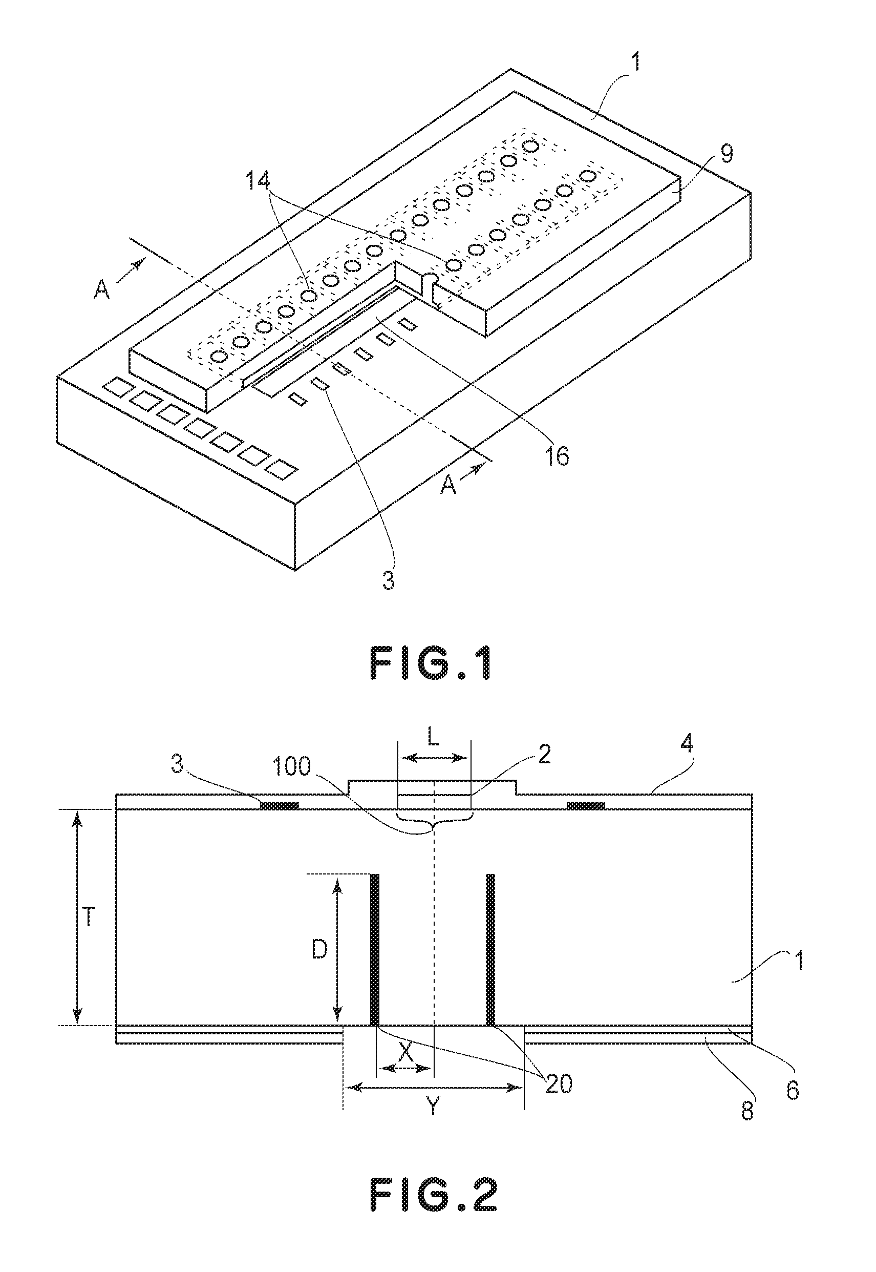
[0038]FIG. 1 shows a part of the ink jet recording head in this embodiment of the present invention.

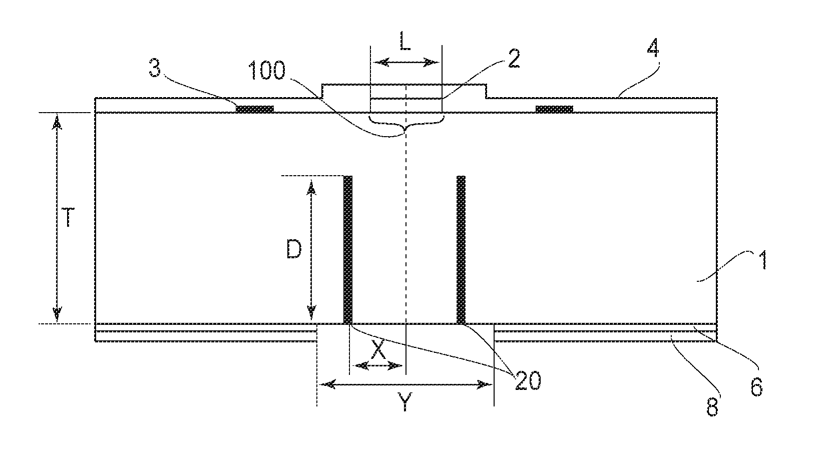
[0039]This ink jet recording head (liquid jetting head) has a silicon substrate 1, which has two rows of elements 3 for generating ink (liquid) jetting energy (which hereafter may be referred to simply as energy generation elements). In each row, the energy generation elements are aligned with a preset pitch. The silicon substrate 1 is covered with a layer of polyether-amide (unshown) as an adhesion enhancement layer. Also located on the silicon substrate 1 (adhesion enhancement layer) are a photosensitive resin layer 9, which is the layer through which ink jetting holes 14 (liquid jetting hole) are formed. The ink jet holes 14 are located above the energy generation elements 3, one for one. This photosensitive layer 9 also serves as the top wall of each ink passage which leads from the common ink delivery channel 16 (liquid delivery hole) to ink jetting hole 14. In terms of the direc...

embodiment 2

[0081]FIG. 7 is a sectional view of the ink jet recording head chip in the second embodiment of the present invention.

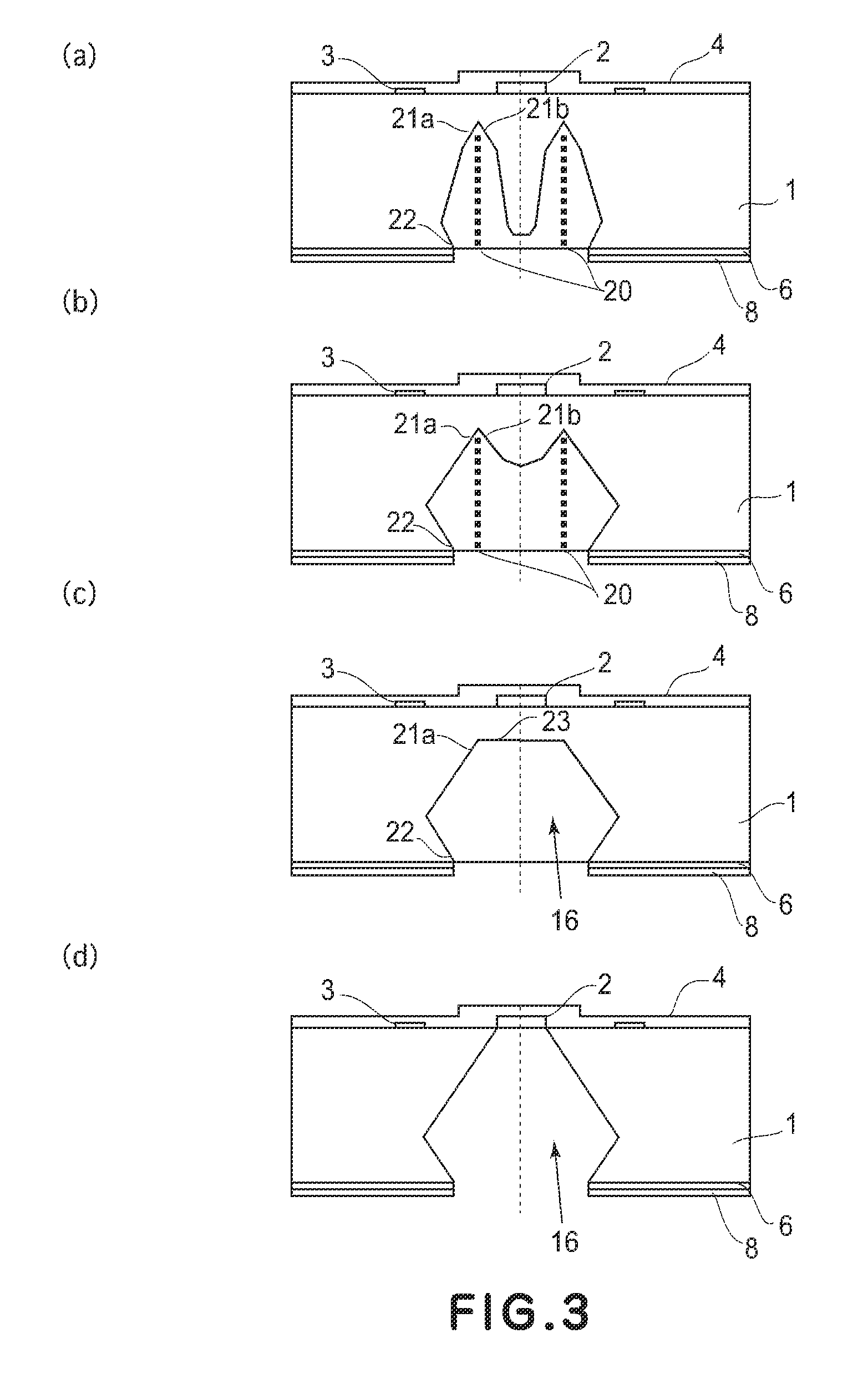
[0082]The ink jet recording head chip in this embodiment is provided with multiple common ink delivery channels, which were formed in parallel with the use of the manufacturing method in the first embodiment described above. Thus, each common ink delivery channel 16 of the ink jet recording head chip in this embodiment also has the “”-shaped cross section.

[0083]FIG. 8 is a sectional view of an ink jet recording head chip formed with the use of an ink jet head manufacturing method in accordance with the prior art, which does not use pilot holes to form the common ink delivery channels. As will be evident from the comparison between FIGS. 7 and 8, the ink jet recording head chip manufacturing method in this embodiment used for forming the ink jet recording head chip shown in FIG. 7, makes it possible to form the common ink delivery channel 16, the width of which on the...


PUM

PropertyMeasurementUnit
thicknessaaaaaaaaaa
wavelengthaaaaaaaaaa
diameteraaaaaaaaaa

Abstract

A manufacturing method for a substrate for an ink jet head, including formation of an ink supply port in a silicon substrate, the method includes a step of forming, on one side of the substrate, an etching mask layer having an opening at a position corresponding ink supply port; a step of forming unpenetrated holes through the opening of the etching mask layer in at least two rows in a longitudinal direction of the opening; and a step of forming the ink supply port by crystal anisotropic etching of the substrate in the opening.

Description

FIELD OF THE INVENTION AND RELATED ART[0001]The present invention relates to a manufacturing method for an ink jet recording head chip recording on recording medium by jetting ink, and a manufacturing method for an ink jet recording head.[0002]Ink jet heads of the type which jet ink upward of the elements for generating the ink jetting pressure have long been known (hereafter, this type of ink jet head may be referred to as side shooter head). This type of ink jet head is provided with a substrate, and an ink jetting energy generating portions which are on one of the primary surfaces of the substrate. The ink jetting energy generating portions are supplied with ink, from the back side, that is, the opposite surface of the substrate from the surface having the ink jetting energy generating portions, through the through holes.[0003]One of the manufacturing methods for this type of ink jet head is disclosed in U.S. Pat. No. 6,143,190. More specifically, this patent discloses an ink jet...

Claims


Application Information

Patent Timeline
Patent Type & Authority Patents(United States)
IPC IPC(8): B41J2/16
CPCB41J2/1603B41J2/1628B41J2/1631B41J2/1632B41J2/1634B41J2/1635B41J2/1639B41J2/1645H01L21/76898
Inventor SAKAI, TOSHIYASUKOYAMA, SHUJIONO, KENJIYAMAMURO, JUN
Owner CANON KK
Why Eureka
Try Eureka