Multi-die DC-DC buck power converter with efficient packaging

a buck power converter and buck power supply technology, applied in the field of physical level packaging of switching power supply and dcdc voltage converter, can solve the problems of increased demand for different voltage levels, non-standard lead frame, and large package siz

Active Publication Date: 2010-11-02
ALPHA & OMEGA SEMICON LTD
View PDF24 Cites 5 Cited by
  • Summary
  • Abstract
  • Description
  • Claims
  • Application Information

AI Technical Summary

Benefits of technology

[0012]In one embodiment, the Schottky diode is placed on the die pad side by side with the vertical MOSFET with the cathode of the Schottky diode electrically connected to the source of the vertical MOSFET via the first die pad. Correspondingly, the PRC die can be attached atop the first die pad via an insulating die bonding material to achieve a further reduced footprint of the first die pad with the Schottky diode, the vertical MOSFET and the PRC co-packaged atop the first die pad. As an alternative trade-off, a second die pad is provided on the lead-frame and the PRC die can be attached to the second die pad via a standard conductive die bonding material.
[0013]In an alternative embodiment the first die pad is grounded. Correspondingly, the vertical MOSFET is a vertical N-channel FET, the top of the Schottky diode die is its cathode and the bottom of the vertical MOSFET is its source. The Schottky diode die and the vertical MOSFET die are co-packaged atop the first die pad in a stacked way with the vertical MOSFET die atop the Schottky diode die for minimized vertical MOSFET source inductance, minimized Schottky diode anode inductance and easy heat sinking. With the first die pad grounded, the PRC die can be attached atop the first die pad via a standard conductive die bonding material to achieve a further reduced footprint of the first die pad with the Schottky diode, the vertical MOSFET and the PRC co-packaged atop the first die pad.
[0015]For applications where both the unregulated DC input and the regulated DC output are negative voltages hence the vertical MOSFET is a vertical P-channel FET, the Schottky diode die is supplied with its bottom being its anode while the bottom of the vertical MOSFET being its source. The Schottky diode die and the vertical MOSFET die are then co-packaged side by side atop the first die pad. Correspondingly, the PRC die is attached atop the first die pad via an insulating die bonding material to achieve a further reduced footprint of the first die pad with the Schottky diode, the vertical MOSFET and the PRC co-packaged atop the first die pad. As an alternative trade-off, a second die pad is provided on the lead-frame and the PRC die can be attached to the second die pad via a standard conductive die bonding material.
[0016]For applications where both the unregulated DC input and the regulated DC output are negative voltages hence the vertical MOSFET is a vertical P-channel FET, the first die pad can be grounded. Correspondingly, the Schottky diode die can be supplied with its substrate being its cathode while the bottom of the vertical MOSFET being its source. The Schottky diode die and the vertical MOSFET die are co-packaged atop the first die pad in a stacked way with the vertical MOSFET die atop the Schottky diode die for minimized vertical MOSFET source inductance, minimized Schottky diode anode inductance and easy heat sinking. With the first die pad grounded, the PRC die can be attached atop the first die pad via a standard conductive die bonding material to achieve a further reduced footprint of the first die pad with the Schottky diode, the vertical MOSFET and the PRC co-packaged atop the first die pad.

Problems solved by technology

Also, due to increased complexities and features of portable devices, there is an increased demand for different voltage levels within one portable device.
As a minimum clearance between the two isolated die pads (Schottky diode die pad 30c and MOSFET die pad 31c) must be maintained for isolation and product reliability, this results in a larger package size and the use of non-standard lead frame thus leads to higher cost.
The required bond wires 34a further increases the cost of the package.
Additionally, the bond wires 34a, owing to their associated parasitic capacitance and inductance, can also cause a degradation of the power conversion efficiency of the boost power converter.

Method used


Image

  • Multi-die DC-DC buck power converter with efficient packaging
  • Multi-die DC-DC buck power converter with efficient packaging
  • Multi-die DC-DC buck power converter with efficient packaging

Examples


first embodiment

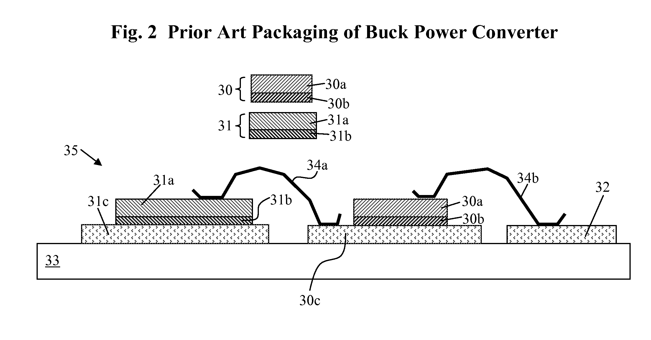
[0026]FIG. 3A (side view), FIG. 3B (top view) and FIG. 3C (top view) illustrate the present invention multi-die package 45 and 45a with Schottky diode 30 and the vertical MOSFET 51 enclosed in molding compound 49. Compared with the prior art multi-die package 35 of FIG. 2 that uses two die pads (Schottky diode die pad 30c and MOSFET die pad 31c), the present invention only needs a lead-frame with first die pad 40c for packaging both the Schottky diode 30 and the vertical MOSFET 51 into one package to be mounted onto a PC-board 43. While the die-level device terminal configuration for the Schottky diode is the same between FIG. 2 and FIG. 3A (bottom substrate=cathode 30b, top surface=anode 30a), the die-level device terminal configuration for the vertical MOSFET is reversed between FIG. 2 and FIG. 3A in that:

[0027]FIG. 2: bottom substrate=MOSFET drain 31b, top surface=MOSFET source and gate 31a

[0028]FIG. 3A: bottom substrate=MOSFET source 52a, top surface=MOSFET gate and drain 52b

[...

second embodiment

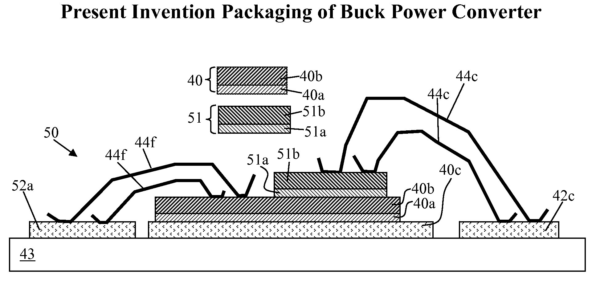
[0031]FIG. 4A (side view), FIG. 4B (top view) and FIG. 4C (top view) illustrate the present invention multi-die package 50 and 50a with Schottky diode 40 and the vertical MOSFET 51 enclosed in molding compound 49. Compared with the previous present invention multi-die package 45 of FIG. 3A, the die-level device terminal configuration for vertical MOSFET is the same between FIG. 3A and FIG. 4A (bottom substrate=MOSFET source 51a, top surface=MOSFET gate and drain 51b). However, the die-level device terminal configuration for the Schottky diode is reversed between FIG. 3A and FIG. 4A in that:

[0032]FIG. 3A: bottom substrate=Schottky diode cathode 30b, top surface=Schottky diode anode 30a

[0033]FIG. 4A: bottom substrate=Schottky diode anode 40a, top surface=Schottky diode cathode 40b

[0034]As noted in FIG. 2B, the Schottky diode 30 die typically comes with its cathode 30b as the bottom substrate and its anode 30a on the top. Hence, to realize the various embodiments of the present inven...

third embodiment

[0036]FIG. 5A, FIG. 5B, FIG. 5C and FIG. 5D illustrate the present invention multi-die semiconductor package. As noted in FIG. 2 before, the Schottky diode 30 die typically comes with its cathode 30b as the bottom substrate and its anode 30a on the top. Hence, to realize the various embodiments of the present invention wherein the bottom substrate of the Schottky diode is its anode the Schottky diode must be custom made accordingly. In fact, reference (B) entitled “BOTTOM ANODE SCHOTTKY DIODE STRUCTURE AND METHOD”, as incorporated herein by reference, describes the structure of such bottom anode Schottky diode and how it can be made. However, as a simple alternative as illustrated in FIG. 5A, the Schottky diode can also be made with a typical process albeit into a flip-chip BGA (ball grid array) style Schottky diode 60 thus packaged with its cathode substrate 60b on the top and its anode solder balls 61 at the bottom. The resulting embodiments 65 and 65a, employing the packaging sch...


PUM


Abstract

A DC-DC buck converter in multi-die package is proposed having an output inductor, a low-side Schottky diode and a high-side vertical MOSFET controlled by a power regulating controller (PRC). The multi-die package includes a first die pad with the Schottky diode placed there on side by side with the vertical MOSFET. The PRC die is attached atop the first die pad via an insulating die bond. Alternatively, the first die pad is grounded. The vertical MOSFET is a top drain N-channel FET, the substrate of Schottky diode die is its anode. The Schottky diode and the vertical MOSFET are stacked atop the first die pad. The PRC is attached atop the first die pad via a conductive die bond. The Schottky diode die can be supplied in a flip-chip configuration with cathode being its substrate. Alternatively, the Schottky diode is supplied with anode being its substrate without the flip-chip configuration.

Description

CROSS REFERENCE TO RELATED APPLICATIONS[0001]This application is a continuation in part (CIP) of the following concurrently filed patent applications:[0002](A) “Bottom Source LDMOSFET Structure and Method”, Ser. No. 11 / 495,803, Jul. 28, 2006, François Hébert, issued on Jun. 30, 2009 as U.S. Pat. No. 7,554,154.[0003](B) Title: “BOTTOM ANODE SCHOTTKY DIODE STRUCTURE AND METHOD” by François Hébert, filed on Jul. 22, 2007 with application Ser. No. 11 / 880,497 and issued on Dec. 15, 2009 as U.S. Pat. No. 7,633,135.[0004](C) Title: “A Multi-die DC-DC Boost Power Converter with Efficient Packaging”, Inventors: Francois Hebert, Allen Chang, Peter Cheng, filed on Jul. 31, 2007 with application Ser. No. 11 / 830,951.whose contents are incorporated herein by reference for any and all purpose.FIELD OF INVENTION[0005]This invention relates generally to the field of electrical power supply and conversion. More specifically, the present invention is directed to the physical level packaging of a switc...

Claims


Application Information

Patent Timeline
Patent Type & Authority Patents(United States)
IPC IPC(8): H01L23/34
CPCH01L23/49562H01L24/49H01L23/49575H01L2924/12032H01L25/16H01L2224/48091H01L2224/48227H01L2224/48247H01L2224/49111H01L2224/49171H01L2224/73265H01L2924/01005H01L2924/01015H01L2924/01027H01L2924/01033H01L2924/01082H01L2924/13091H01L2924/14H01L2924/19041H01L2924/19042H01L2924/30105H01L2924/30107H01L2224/73257H01L2224/16245H01L2924/12041H01L2224/48472H01L2924/014H01L2924/01006H01L2224/32245H01L2224/32145H01L24/48H01L2924/00014H01L2924/00012H01L2924/00H01L2224/32225H01L2924/181H01L24/73H01L2924/00011H01L2224/45099H01L2224/05599H01L2224/0401
Inventor HEBERT, FRANCOISCHANG, ALLEN
Owner ALPHA & OMEGA SEMICON LTD
Why Eureka
Try Eureka