Nitride based semiconductor device with concave gate region

a nitride-based semiconductor and gate region technology, applied in the field of semiconductor devices, can solve the problems of reproducible fabrication of semiconductor devices having a group iii nitride semiconductor, and achieve the effects of reducing the surface state present, reducing the localization of an electric field, and reducing the gate resistan

Active Publication Date: 2010-11-23
PANASONIC CORP
View PDF13 Cites 27 Cited by
  • Summary
  • Abstract
  • Description
  • Claims
  • Application Information

AI Technical Summary

Benefits of technology

[0008]By contrast, in a semiconductor device according to the present invention, the occurrence of the current collapse can be suppressed with excellent reproducibility, which will be shown specifically hereinbelow.
[0024]In addition, a film thickness of a portion of the p-type nitride-based compound semiconductor layer located over a bottom surface of the concave portion is preferably larger than a film thickness of a portion of the p-type nitride-based compound semiconductor layer located on the upper surface of the semiconductor multilayer. This makes it possible to reduce the surface states present at the surface of the semiconductor multilayer and further suppress the current collapse.

Problems solved by technology

However, because Japanese Laid-Open Patent Publication No. 2005-210105 does not disclose a specific problem solving method, it is difficult to fabricate a semiconductor device having a group III nitride semiconductor reproducibly.

Method used


Image

  • Nitride based semiconductor device with concave gate region
  • Nitride based semiconductor device with concave gate region
  • Nitride based semiconductor device with concave gate region

Examples


embodiment 1

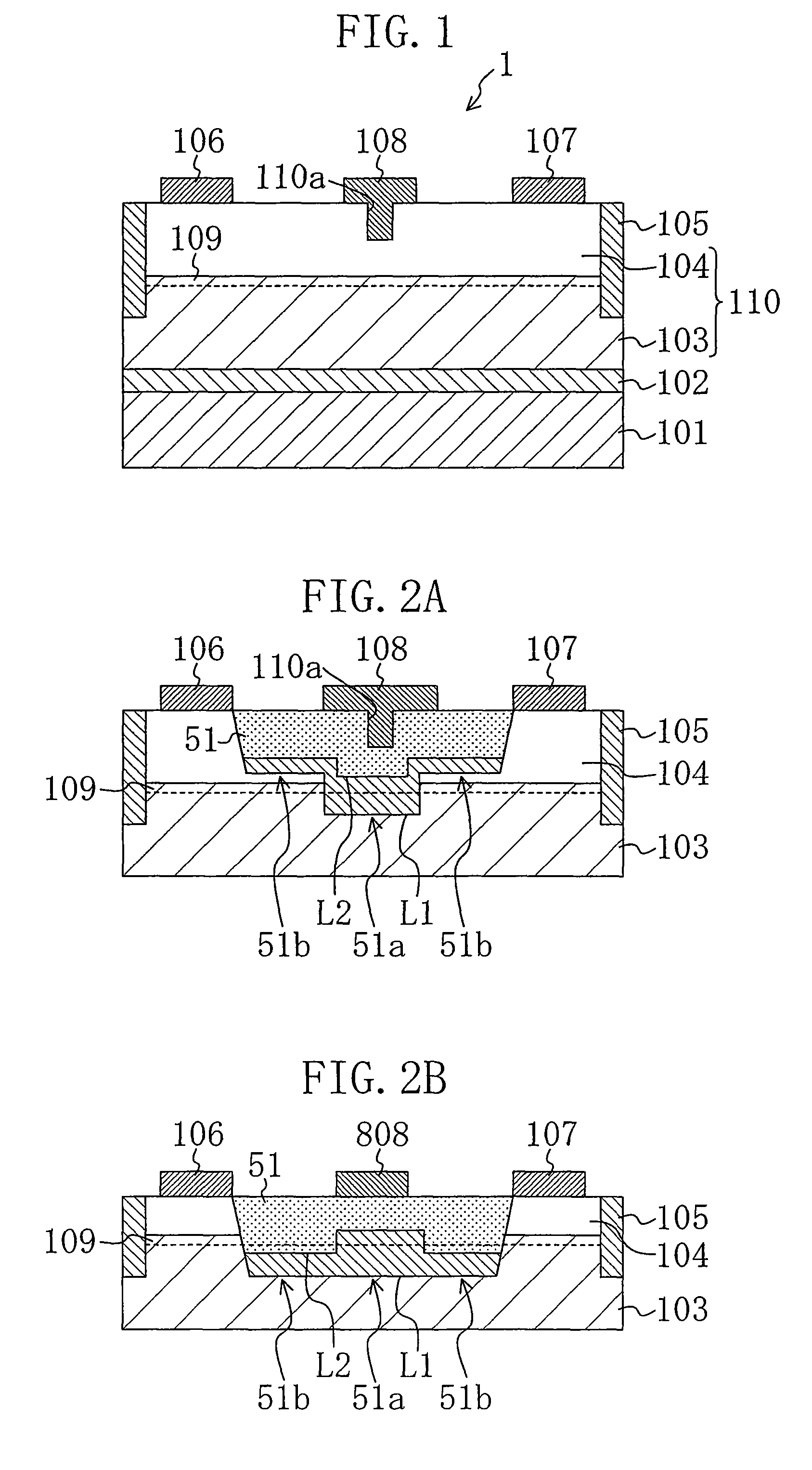
[0050]FIG. 1 is a cross-sectional view showing a structure of a FET 1 according to the first embodiment of the present invention.

[0051]The FET 1 according to the present embodiment comprises: a substrate 101; a buffer layer 102; a first nitride semiconductor layer (first nitride-based compound semiconductor) 103; a second nitride semiconductor layer (second nitride-based compound semiconductor layer) 104; isolation regions 105; a source electrode 106; a drain electrode 107; and a gate electrode 108. In the second nitride semiconductor layer 104, a concave portion 110a is formed to be concaved in the thickness direction of the second nitride semiconductor layer 104.

[0052]Specifically, as shown in FIG. 1, the buffer layer 102, the first nitride semiconductor layer 103, and the second nitride semiconductor layer 104 are successively stacked on the substrate 101. The first nitride semiconductor layer 103 and the second nitride semiconductor layer 104 constitute a semiconductor multilaye...

embodiment 2

[0081]FIG. 7 is a cross-sectional view showing a structure of a FET 11 according to the second embodiment of the present invention.

[0082]The FET 11 according to the present embodiment is different from the FET 1 according to the first embodiment in that a p-type nitride semiconductor layer 117 is provided between the lower surface of a gate electrode 118 and the bottom surface of the concave portion 110a. Specifically, the p-type nitride semiconductor layer 117 is provided in the concave portion 110a and also on the upper surface of the second nitride semiconductor layer 104. In other words, the portion of the p-type nitride semiconductor layer 117 located over the bottom surface of the concave portion 110a is thicker than the portion of the p-type nitride semiconductor layer 117 provided on the upper surface of the second nitride semiconductor layer 104. The gate electrode 118 is provided on the upper surface of the p-type nitride semiconductor layer 117. In such a structure also, ...

embodiment 3

[0105]FIG. 15 is a cross-sectional view showing a structure of a FET 2 according to the third embodiment of the present invention.

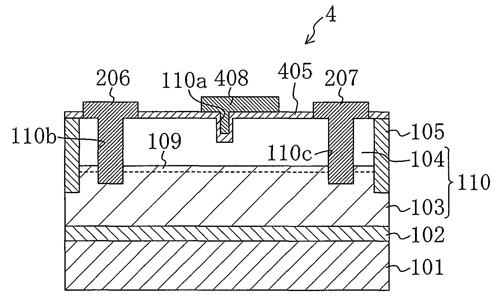
[0106]In the FET 2 according to the present embodiment, an insulating film 205 is provided on the upper surface of the second nitride semiconductor layer 104, and a source electrode 206, a drain electrode 207, and a gate electrode 208 are provided on the upper surface of the second nitride semiconductor layer 104. The gate electrode 208 is formed such that the portion thereof provided on the upper surface of the second nitride semiconductor layer 104 is asymmetrical with respect to the center axis of the bottom surface of the concave portion 110a. Moreover, the source electrode 206 and the drain electrode 207 extend through the second nitride semiconductor layer 104. In the description given hereinbelow, portions different from those of the foregoing first embodiment will be primarily shown.

[0107]As shown in FIG. 15, in the FET 2 according to the present ...


PUM


Abstract

In FET, a second nitride semiconductor layer is provided on a first nitride semiconductor layer, and a source electrode and a drain electrode are each provided to have at least a portion thereof in contact with the second nitride semiconductor layer. A concave portion is formed in the upper surface of the second nitride semiconductor layer to be located between the source electrode and the drain electrode. A gate electrode is provided over the concave portion to cover the opening of the concave portion.

Description

BACKGROUND OF THE INVENTION[0001]The present invention relates to a semiconductor device and a method for fabricating the same and, more particularly, to a semiconductor device having a nitride-based compound semiconductor layer and a method for fabricating the same.[0002]A Group III nitride-based compound semiconductor (hereinafter referred to as “Group III nitride semiconductor”) represented by gallium nitride (GaN) shows a breakdown field and a saturation electron velocity which are higher than those shown by silicon (Si) and gallium arsenide (GaAs). Therefore, a field effect transistor (hereinafter abbreviated as “FET”) using a group III nitride semiconductor is regarded as promising as a next-generation high-frequency device or high-power switching device and has been widely investigated.[0003]In general, high-density trap states (surface states) exist at a surface of a group III nitride semiconductor so that carriers are trapped. Because of this, when a switching device, e.g.,...

Claims


Application Information

Patent Timeline
Patent Type & Authority Patents(United States)
IPC IPC(8): H01L29/778
CPCH01L29/1029H01L29/1066H01L29/42316H01L29/66462H01L29/7787H01L29/2003H01L29/41766H01L29/4236
Inventor NAKAZAWA, KAZUSHINAKAZAWA, SATOSHIUEDA, TETSUZOTANAKA, TSUYOSHIHIKITA, MASAHIRO
Owner PANASONIC CORP
Why Eureka
Try Eureka