
ZQ calibration circuit and a semiconductor device including a ZQ calibration circuit

a calibration circuit and semiconductor technology, applied in the field of semiconductor devices including zq calibration circuits, can solve the problems of inability to perform high-speed data transfer, inability to guarantee the impedance adjustment, and the impedance of the transmission line not matching the output impedance, so as to achieve more accurate impedance adjustment, increase the number of impedance adjustments, and increase the effect of impedance adjustmen

Active Publication Date: 2010-11-23
LONGITUDE LICENSING LTD
View PDF19 Cites 36 Cited by
  • Summary
  • Abstract
  • Description
  • Claims
  • Application Information

AI Technical Summary

Benefits of technology

The present invention provides a ZQ calibration circuit and a semiconductor device with the circuit that can automatically adjust the impedance of a transmission line and the output impedance of a semiconductor device for more accurate impedance matching. This is achieved by adding a ZQ calibration operation during a self-refresh operation, which increases the number of impedance adjustments and allows for faster data transfer. The ZQ calibration circuit uses a different control signal than an externally inputted ZQ calibration command, and includes a pull-up circuit, a pull-down circuit, and comparators to perform the calibration operation. The semiconductor device with the ZQ calibration circuit can perform high-speed data transfer.

Problems solved by technology

If the impedance of the transmission lines between the semiconductor devices and the output impedance of the semiconductor device are not matched with each other, then a data waveform is dulled during transmission so as to cause an overshoot or an undershoot, so that a high speed data transfer cannot be performed.
That is, in a case where a self-refresh operation or the like is performed for a long period of time, even if a short-time ZQ calibration (tZQCS or tZQoper) is performed after the self-refresh operation, there is no guarantee that the impedance can be adjusted.
If the impedance matching is not completed successfully, the impedance of the transmission line does not match the output impedance of the semiconductor device.
In this case, a data waveform is dulled during transmission so as to cause an overshoot or an undershoot, so that a high speed data transfer cannot be performed.
In this case, the impedance of the transmission line does not match the output impedance of the semiconductor device.
As a result, a data waveform is dulled during transmission so as to cause an overshoot or an undershoot, so that a high speed data transfer cannot be performed.

Method used


Image

  • ZQ calibration circuit and a semiconductor device including a ZQ calibration circuit
  • ZQ calibration circuit and a semiconductor device including a ZQ calibration circuit
  • ZQ calibration circuit and a semiconductor device including a ZQ calibration circuit

Examples


Embodiment Construction

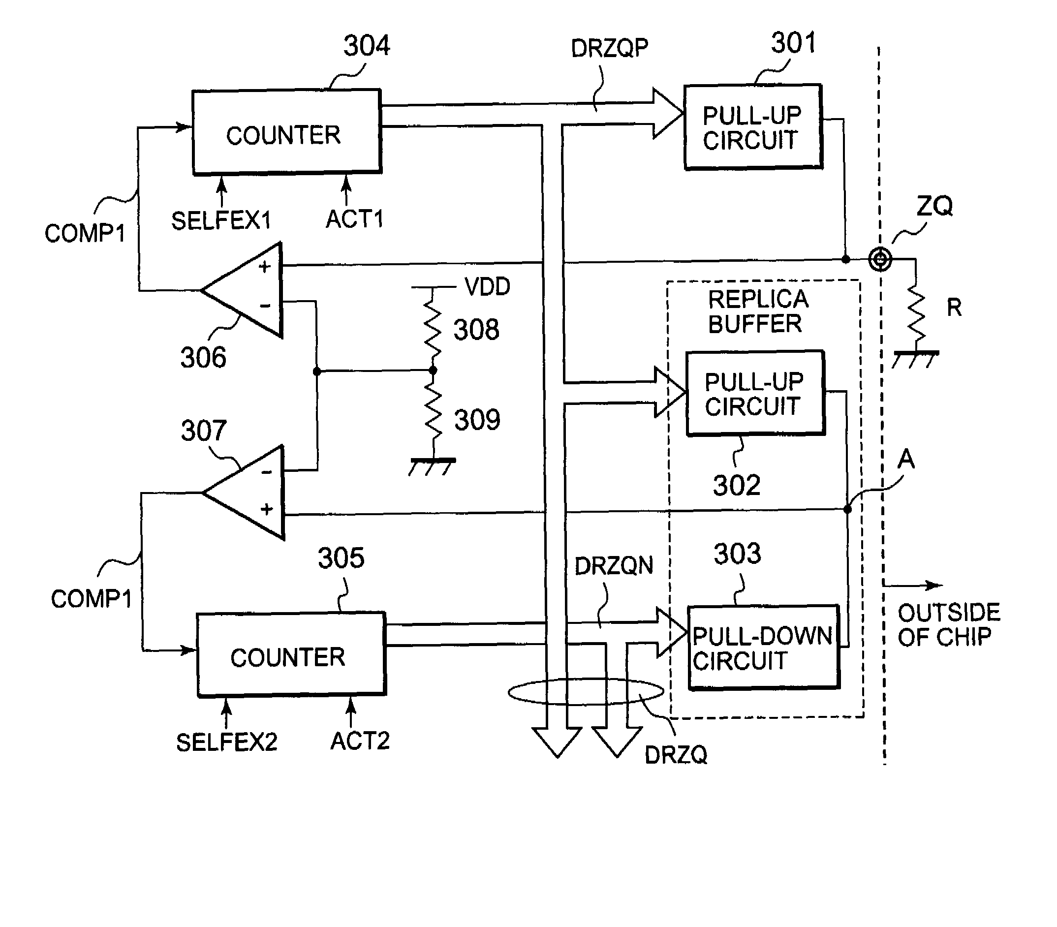
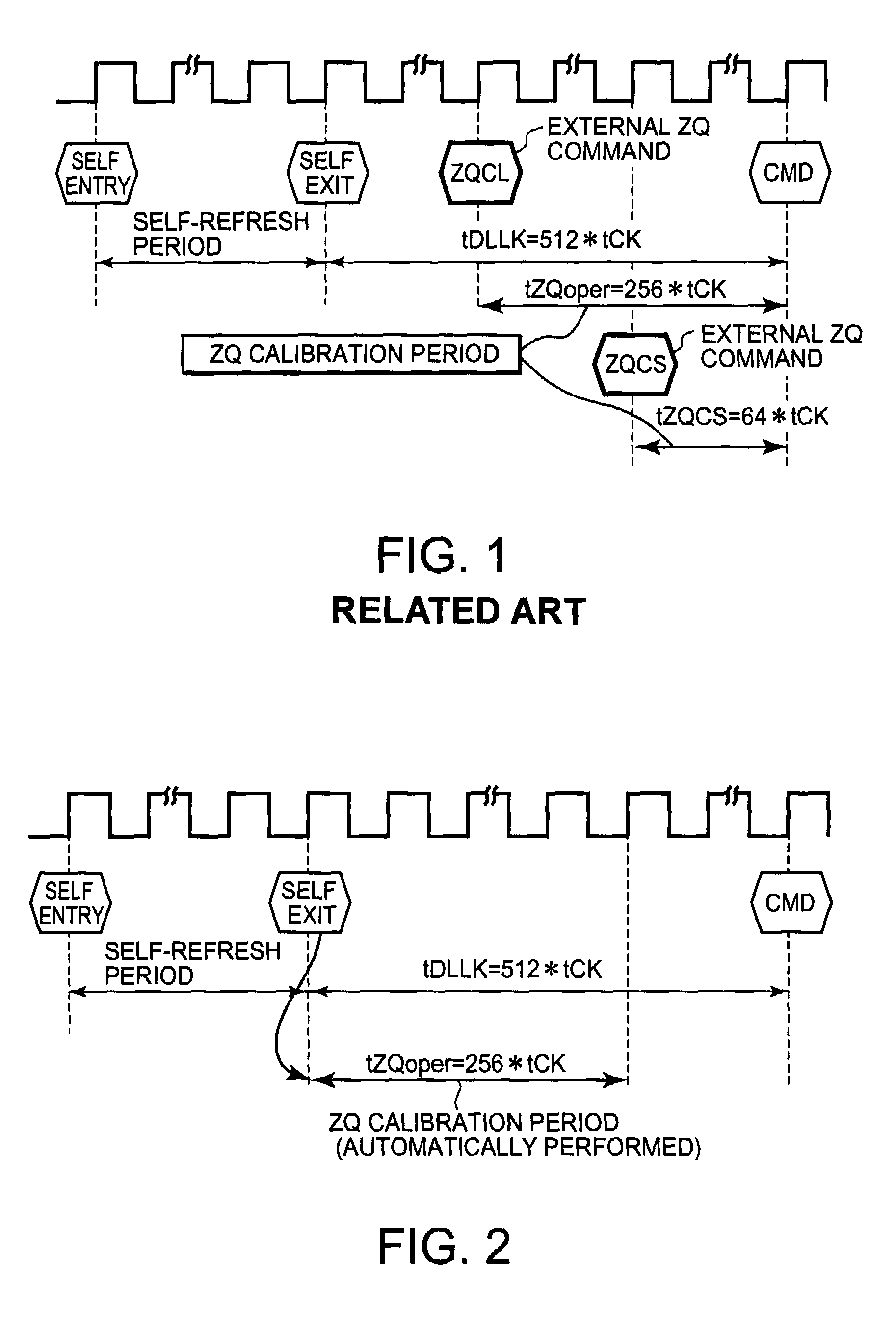
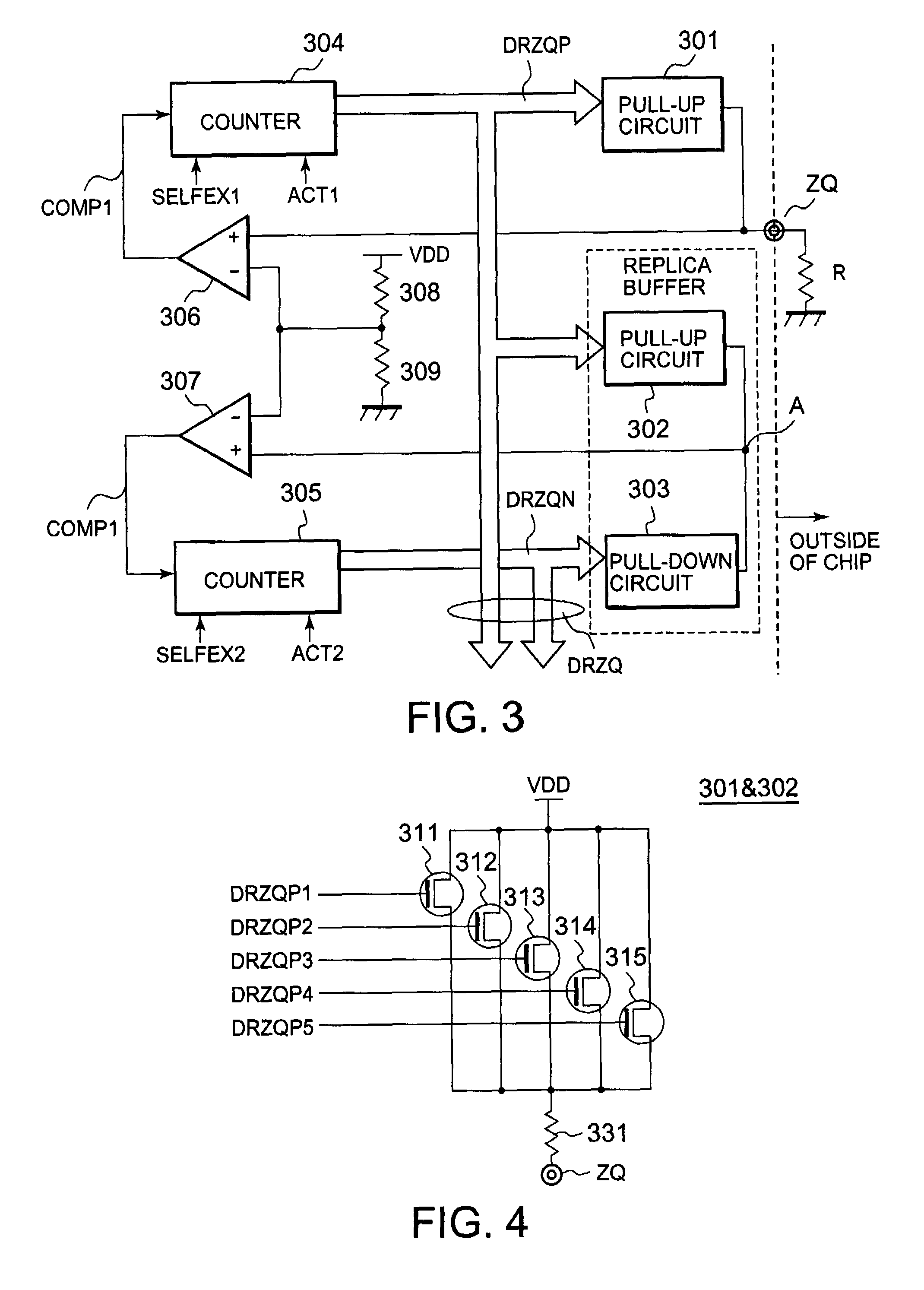
[0029]A preferred embodiment of the present invention will be described below with reference to FIGS. 2 through 6. FIG. 2 is a timing chart of a ZQ calibration operation according to the present invention. FIG. 3 is a circuit diagram of a ZQ calibration circuit, FIG. 4 is a circuit diagram of a pull-up circuit, and FIG. 5 is a circuit diagram of a pull-down circuit. FIG. 6 is a timing chart of a ZQ calibration operation. As shown in FIG. 2, the ZQ calibration circuit according to the present invention automatically performs a ZQ calibration operation after completion of a self-refresh operation. Even if no external ZQ calibration command is inputted, the ZQ calibration circuit automatically performs a ZQ calibration operation after completion of the self-refresh operation. Specifically, the ZQ calibration circuit concurrently performs a ZQ calibration operation (tDQoper=256*tCK) within a DLL clock cycle (tDLLK=512*tCK) after completion of the self-refresh operation.

[0030]The ZQ cali...


PUM


Abstract

A ZQ calibration command is internally generated from an external command different from a ZQ calibration command so as to automatically perform an additional ZQ calibration operation. A command interval between an inputted command and a next command is effectively employed to obtain a ZQ calibration period. The external command different from the ZQ calibration command is preferably a self-refreshed command. The addition of the ZQ calibration operation shortens intervals between ZQ calibration operations. Thus, it is possible to obtain a ZQ calibration circuit capable of performing a ZQ calibration operation more accurately.

Description

[0001]This application claims priority to prior Japanese patent application JP 2005-309416, the disclosure of which is incorporated herein by reference.BACKGROUND OF THE INVENTION[0002]1. Field of the Invention[0003]The present invention relates to a semiconductor device, and more particularly to a ZQ calibration circuit for adjusting impedance of an output circuit and a semiconductor device having such a ZQ calibration circuit.[0004]2. Description of the Related Art[0005]The speed of recent electronic systems has been enhanced, and an extremely high data transfer rate has been achieved between semiconductor devices forming a system. In order to achieve such an ultrafast data transfer, the amplitude of data signals is reduced. Further, impedance of a transmission line between semiconductor devices and an output impedance of an output circuit of the semiconductor device are matched with each other. The matched impedance provides transmission without causing distortion to data signals...

Claims


Application Information

Patent Timeline
Patent Type & Authority Patents(United States)
IPC IPC(8): G01R31/26
CPCG11C7/1051G11C7/1057H04L25/0278G11C2207/2254G11C11/40615G11C11/4096
Inventor NAKAMURA, MASAYUKIYOKO, HIDEYUKI
Owner LONGITUDE LICENSING LTD
Learn More