Electron optical apparatus, X-ray emitting device and method of producing an electron beam

a technology of electron beam and optical apparatus, applied in the direction of electrical apparatus, x-ray tube details, electric discharge tubes, etc., can solve the problems of tube size limitation, achieve the effect of short length, save space, and improve the focus of electron beam

Active Publication Date: 2010-11-23
KONINKLIJKE PHILIPS ELECTRONICS NV
View PDF15 Cites 44 Cited by
  • Summary
  • Abstract
  • Description
  • Claims
  • Application Information

AI Technical Summary

Benefits of technology

[0010]This aspect of the invention is based on the idea to combine into an electron optical apparatus the advantages of a double quadrupole lens consisting of a first magnetic quadrupole lens and a second magnetic quadrupole lens and the advantages of a thin, flat and unstructured or only slightly structured emitter. The double quadrupole provides excellent focusing properties. The flat emitter having a planar surface for emitting electrons provides for a reduced lateral energy component of the emitted electrons thereby also contributing to excellent focusing properties of the electron optical apparatus. Furthermore, to fulfill the requested variable focus spot position, a magnetic dipole lens is provided for deflecting the emitted electrons in transversal and radial directions.
[0015]With conventional cathodes including e.g. tungsten coils or flat tungsten emitters with slits the non-planar structure of the cathode heavily distorts the electric potential between the cathode and the anode thereby increasing the velocity component of electrons transverse to the optical axis and hence increasing the focal spot size of the electron optical apparatus.
[0024]According to a an embodiment of the invention the magnetic dipole lens comprises dipole coils which are arranged on the yoke of the second magnetic quadrupole lens. By arranging the dipole coils on this second yoke the magnetic dipole field can be directly superimposed to the magnetic quadrupole field of the second quadrupole lens. The second yoke can serve both as a yoke for the second quadrupole lens and as a yoke for the dipole lens. Thereby space can be saved and the length of the entire electron optical apparatus can be reduced. Furthermore the weight for an additional yoke can be saved.
[0029]According to a further embodiment of the invention the planar surface of the emitter is non-structured. In other words, the surface of the emitter from which the electrons can be emitted towards the anode is a homogeneous plane without any recesses or protrusions. Electrons can be emitted homogeneously from such non-structured surface. Furthermore, such non-structured emitter surface does not disturb the electric field between the cathode including the emitter and the anode. Especially the electric field close to the surface of the emitter is not disturbed by any structures. Accordingly, electric field lines remain linear and electrons are accelerated parallely to the optical axis without any substantial transversal moving component. The electron beam is not widened. This can help in better focusing of the electron beam.
[0030]According to a further embodiment of the invention the planar surface of the emitter is finely structured. In other words, fine structures such as e.g. grooves, slits or recesses are located within the planar surface of the emitter. These fine structures can be used e.g. for confining an electrical current within the emitter which is used to electrically heat the emitter. However, the size and / or arrangement of such fine structures can be chosen such that the emitted electrons are not excessively scattered and such that the electric field is not excessively distorted.
[0034]According to a further embodiment of the invention the electrical anode and the anode disc (=target) are essentially on the same electric potential. In case that a scattered electron collector is provided also this SEC can be set on the electrical potential of the anode. Accordingly, the region between the anode and the anode disc can be free of any electric field. By eliminating any electric field in the proximity of the surface of the anode disc it can be prevented that backscattered electrons coming from the surface of the anode disc are reattracted towards the anode disc. Otherwise, these reattracted backscattered electrons would unnecessarily widen the focal spot and would furthermore contribute to heating of the anode disc thereby increasing the cooling requirements for the anode disc.

Problems solved by technology

Additionally limitations in the tube size with an optical length of 1<130 mm have to be taken into account.
Image quality issues in CT or CV imaging require the possibility of an active control of the focal spot size during image acquisition.

Method used


Image

  • Electron optical apparatus, X-ray emitting device and method of producing an electron beam
  • Electron optical apparatus, X-ray emitting device and method of producing an electron beam
  • Electron optical apparatus, X-ray emitting device and method of producing an electron beam

Examples


Embodiment Construction

[0050]The illustration in the drawing is schematically. It is noted that in different figures, similar or identical elements are provided with the same reference signs or with reference signs, which are different from the corresponding reference signs only within the first digit.

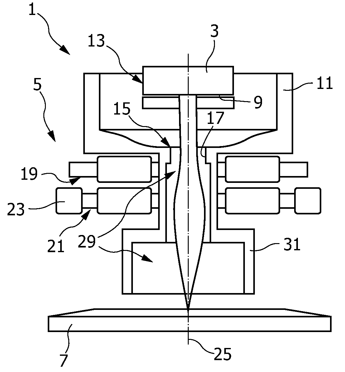
[0051]Future X-ray medical examinations have sophisticated requirements on the spot sizes and shapes in combination with fast changes in positions. Due to the limitations in space of typically 130 mm in optical length and an optimal heat management by implementing a SEC, a much better electron optic than usually used in X-ray tubes is necessary.

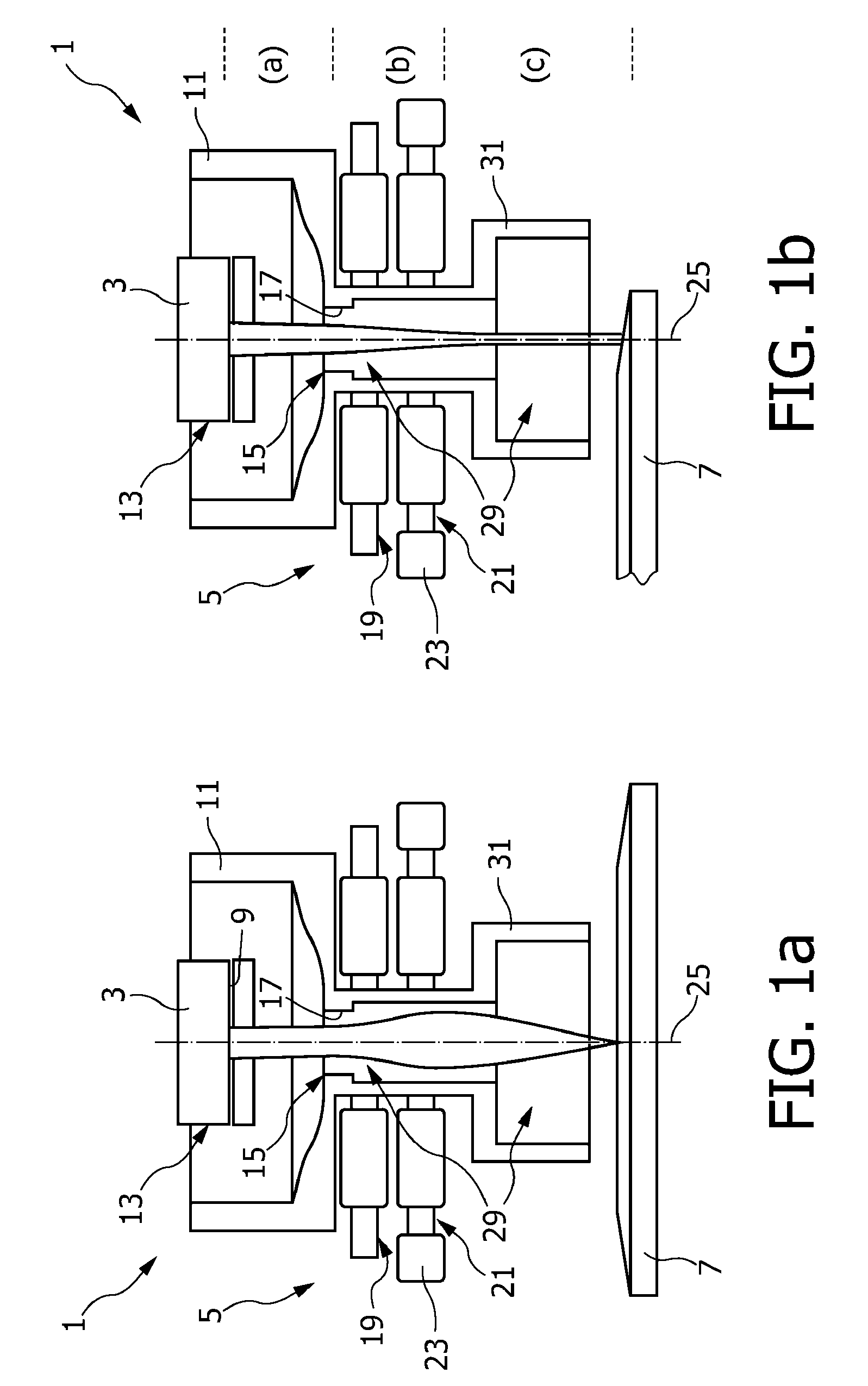
[0052]FIGS. 1a and 1b show an embodiment of an X-ray emitting device 1 according to the invention. The proposed X-ray emitting device to reach the above requirements comprises a cathode with a flat emitter 3 as an electron source and a lens system 5.

[0053]The objective of spot control is to create a line focus (an elongated spot) on the slanted part of an anode disc 7...


PUM


Abstract

It is described an electron optical arrangement, a X-ray emitting device and a method of creating an electron beam. An electron optical apparatus (1) comprises the following components along an optical axis (25): a cathode with an emitter (3) having a substantially planar surface (9) for emitting electrons; an anode (11) for accelerating the emitted electrons in a direction essentially along the optical axis (25); a first magnetic quadrupole lens (19) for deflecting the accelerated electrons and having a first yoke (41); a second magnetic quadrupole lens (21) for further deflecting the accelerated electrons and having a second yoke (51); and a magnetic dipole lens (23) for further deflecting the accelerated electrons.

Description

FIELD OF THE INVENTION[0001]The present invention relates to an electron optical apparatus for producing an electron beam, to an X-ray emitting device and to a method of producing an electron beam.TECHNICAL BACKGROUND[0002]The future demands for high-end computer tomograph (CT) and cardiovascular (CV) imaging regarding the X-ray source are (1) higher power / tube current, (2) smaller focal spots combined with the ability of active control of the size, ratio and position of the focal spot, (3) shorter times for cooling down, and, concerning CT, (4) shorter gantry rotation times. In addition to this, the tube design is limited in length and weight to achieve an easy handling for CV applications and a realisable gantry setup for CT applications.[0003]One key to reach higher power and faster cooling is given by using a sophisticated heat management concept inside the X-ray tube. In conventional bipolar X-ray tubes about 40% of the thermal load of the target is due to electrons backscatter...

Claims


Application Information

Patent Timeline
Patent Type & Authority Patents(United States)
IPC IPC(8): H01J35/30H01J35/14
CPCH01J35/14H01J35/153H01J35/147H01J35/30
Inventor HAUTTMANN, STEFANMARING, WOLFRAMHOLZAPFEL, STEFFEN
Owner KONINKLIJKE PHILIPS ELECTRONICS NV
Why Eureka
Try Eureka