Manufacturing method of wiring substrate and manufacturing method of semiconductor device

a manufacturing method and semiconductor technology, applied in the direction of waveguide devices, substantially flat resonant elements, resonant antennas, etc., can solve the problems of increasing the manufacturing cost of the wiring substrate 301 cannot be reduced, and the difficulty of improving the productivity of the wiring substrate, etc., to achieve the effect of reducing the manufacturing cost of the semiconductor device and miniaturizing the wiring substra

Active Publication Date: 2010-11-30
SHINKO ELECTRIC IND CO LTD
View PDF14 Cites 18 Cited by
  • Summary
  • Abstract
  • Description
  • Claims
  • Application Information

AI Technical Summary

Benefits of technology

[0012]Embodiments of the present invention provide a manufacturing method of a wiring substrate capable of reducing a manufacturing cost of a semiconductor device and a wiring substrate miniaturized, and a manufacturing method of a semiconductor device.
[0014]In a related-art manufacturing method of a wiring substrate, a metal plate is used as a support plate in the case of forming the multiplayer wiring structural body by a build-up method in order form a thin wiring substrate, and after forming the multiplayer wiring structural body, the metal plate is removed. However, according to the one or more embodiments of the invention, by patterning a metal plate used as a support plate in the case of forming a multilayer wiring structural body and forming an antenna, the need for a step of removing the metal plate after forming the multilayer wiring structural body is eliminated, so that the number of manufacturing steps of a wiring substrate can be reduced, so that a manufacturing cost of the wiring substrate can be reduced.
[0016]According to the one or more embodiments of the invention, by disposing a multilayer wiring structural body formation step of forming multilayer wiring structural bodies on pasted first and second metal plates and an antenna formation step of patterning the first and second metal plates and forming antennas in the first and second metal plates, two wiring substrates can be manufactured at once, so that a manufacturing cost of the wiring substrate can be reduced.
[0018]In a related-art manufacturing method of a semiconductor device, a metal plate is used as a support plate in the case of forming the multiplayer wiring structural body by a build-up method in order form a thin wiring substrate, and after forming the multiplayer wiring structural body, the metal plate is removed. However, according to the one or more embodiments of the invention, by patterning a metal plate used as a support plate in the case of forming a multilayer wiring structural body and forming an antenna, the need for a step of removing the metal plate after forming the multilayer wiring structural body is eliminated, so that the number of manufacturing steps of a wiring substrate can be reduced, so that a manufacturing cost of a semiconductor device can be reduced.
[0020]According to the one or more embodiments of the invention, by disposing a multilayer wiring structural body formation step of forming multilayer wiring structural bodies on pasted first and second metal plates and an antenna formation step of patterning the first and second metal plates and forming antennas in the first and second metal plates, two wiring substrates can be manufactured at once, so that a manufacturing cost of a semiconductor device can be reduced.
[0021]One or more embodiments of the present invention may include one or more the following advantages a wiring substrate comprising a multilayer wiring structural body, an antenna and an electronic component disposed in the multilayer wiring structural body, and a semiconductor device comprising the wiring substrate are miniaturized and also, a manufacturing cost of the wiring substrate and the semiconductor device can be reduced.

Problems solved by technology

However, in the related-art manufacturing method of the wiring substrate 301, there were problems in which it is difficult to improve productivity of the wiring substrate 301 and a manufacturing cost of the wiring substrate 301 cannot be reduced.
Consequently, there was a problem of increasing a manufacturing cost of the semiconductor device 300.

Method used


Image

  • Manufacturing method of wiring substrate and manufacturing method of semiconductor device
  • Manufacturing method of wiring substrate and manufacturing method of semiconductor device
  • Manufacturing method of wiring substrate and manufacturing method of semiconductor device

Examples


first embodiment

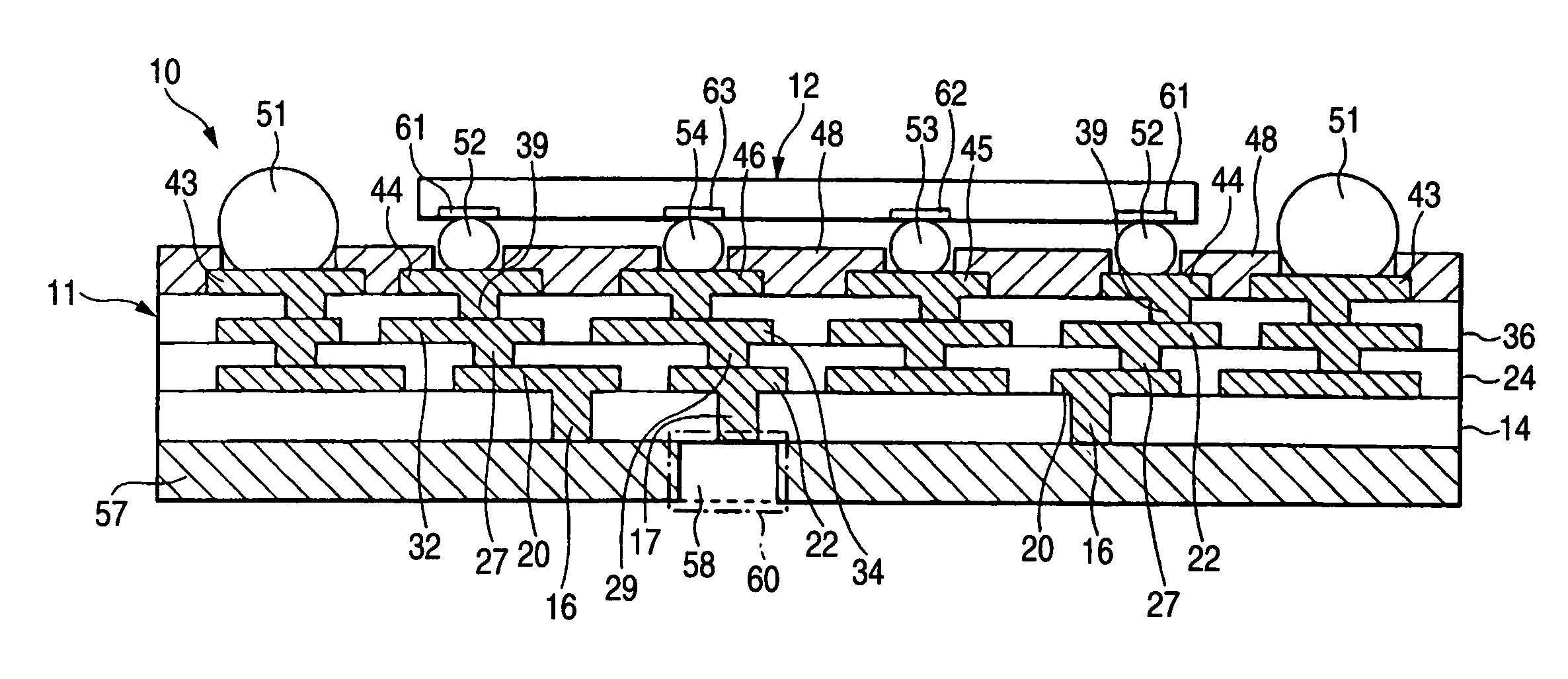
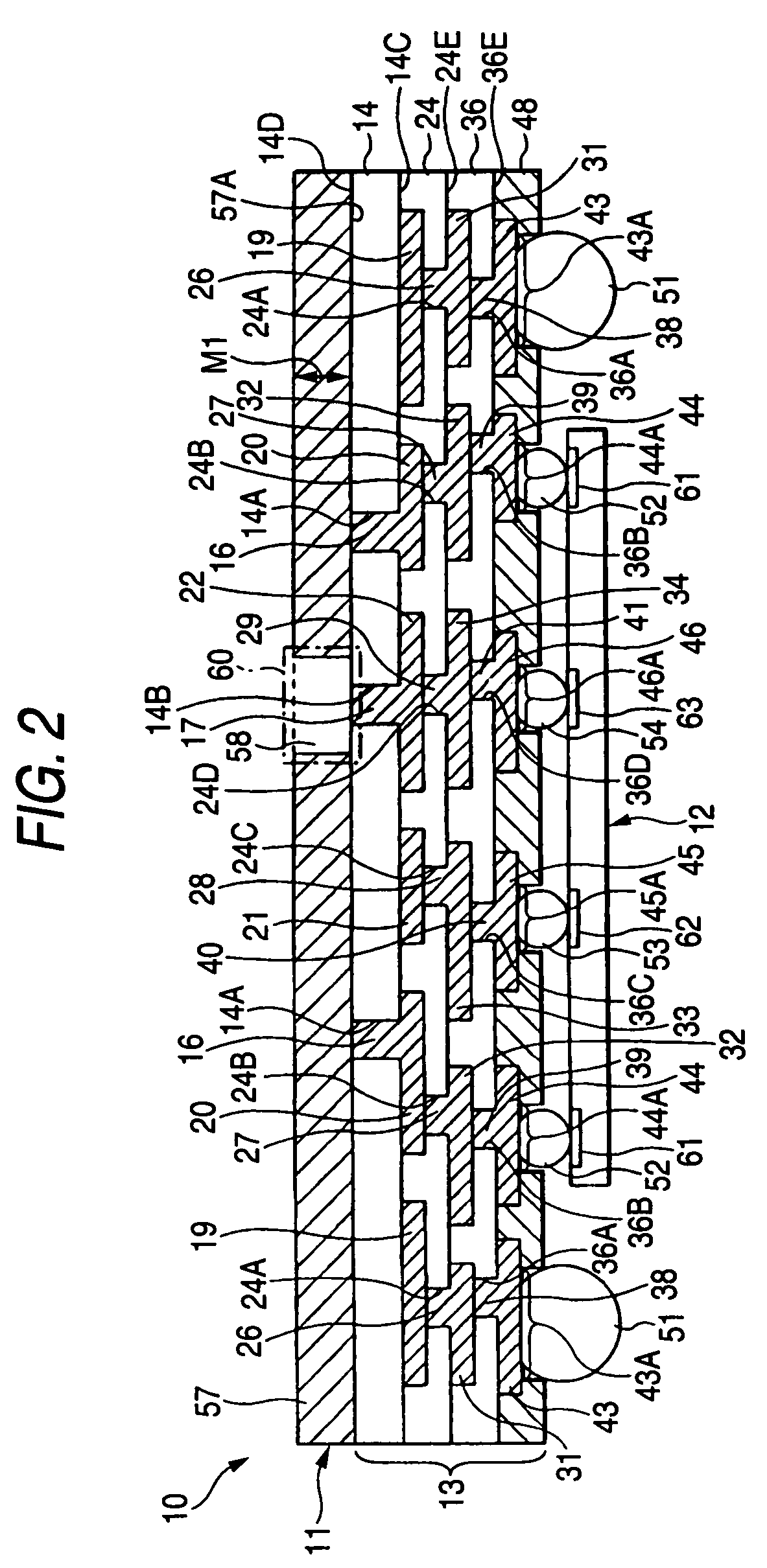
[0062]FIG. 2 is a sectional view of a semiconductor device according to a first embodiment of the invention.

[0063]A semiconductor device 10 of the first embodiment will be described with reference to FIG. 2. In the present embodiment, a semiconductor device used in wireless communication equipment as the semiconductor device 10 will be described as an example.

[0064]The semiconductor device 10 has a wiring substrate 11 and an electronic component 12. The wiring substrate 11 is a coreless substrate, and has a multilayer wiring structural body 13, a first external connection terminal 51, second external connection terminals 52 to 54, a metal plate 57, and a slot antenna 60 which is an antenna.

[0065]The multilayer wiring structural body 13 has insulating layers 14, 24, 36, first vias 16, 17, first wirings 19 to 22, second vias 26 to 29, second wirings 31 to 34, third vias 38 to 41, third wirings 43 to 46, and a protective film 48.

[0066]The insulating layer 14 is disposed so as to cover ...

second embodiment

[0132]FIG. 23 is a sectional view of a semiconductor device according to a second embodiment of the invention.

[0133]A semiconductor device 100 of the second embodiment will be described with reference to FIG. 23. In the present embodiment, a semiconductor device used in wireless communication equipment as the semiconductor device 100 will be described as an example.

[0134]The semiconductor device 100 has a wiring substrate 101 and an electronic component 102. The wiring substrate 101 is a coreless substrate, and has a multilayer wiring structural body 103, a first external connection terminal 151, second external connection terminals 152 to 154, and a patch antenna 160 which is an antenna.

[0135]The multilayer wiring structural body 103 has insulating layers 104, 124, 136, a first via 117, first wirings 118 to 120, a ground layer 121, second vias 126 to 128, second wirings 131 to 134, third vias 138 to 141, third wirings 143 to 146, and a protective film 148.

[0136]The insulating layer...

third embodiment

[0186]FIG. 37 is a sectional view of a semiconductor device according to a third embodiment of the invention. In FIG. 37, the same numerals are assigned to the same component portions as those of the semiconductor device 100 of the second embodiment.

[0187]Referring to FIG. 37, a semiconductor device 180 of the third embodiment is constructed in a manner similar to the semiconductor device 100 except that a metal plate 181 and a circular patch antenna 182 are disposed instead of the patch antenna 160 disposed in the semiconductor device 100 of the second embodiment.

[0188]The metal plate 181 is disposed so as to cover a surface 104C of an insulating layer 104. As the metal plate 181, for example, metal foil can be used. As the metal foil, for example, Cu foil can be used. A thickness M8 of the metal plate 181 (thickness of the circular patch antenna 182) can be set at, for example, 20 to 30 μm.

[0189]FIG. 38 is a diagram viewing the semiconductor device shown in FIG. 37 from the plane....


PUM

PropertyMeasurementUnit
thickness M1aaaaaaaaaa
length L1aaaaaaaaaa
length L1aaaaaaaaaa

Abstract

A multilayer wiring structural body 13 is formed on a surface 57A of a metal plate 57 used as a support plate in the case of forming the multilayer wiring structural body 13, and the metal plate 57 is patterned and a slot antenna 60 is formed.

Description

[0001]This application claims priority to Japanese Patent Application No. 2006-091483, filed Mar. 29, 2006, in the Japanese Patent Office. The priority application is incorporated by reference in its entirety.TECHNICAL FIELD[0002]The present disclosure relates to a manufacturing method of a wiring substrate comprising a multilayer wiring structural body, an antenna and an electronic component disposed in the multilayer wiring structural body, and a manufacturing method of a semiconductor device.RELATED ART[0003]With miniaturization of wireless communication equipment in recent years, miniaturization of a semiconductor device installed in the wireless communication equipment has been desired and the miniaturized semiconductor device includes, for example, a semiconductor device 300 as shown in FIG. 1.[0004]FIG. 1 is a sectional view of a related-art semiconductor device.[0005]Referring to FIG. 1, a related-art semiconductor device 300 has a wiring substrate 301, electronic components...

Claims


Application Information

Patent Timeline
Patent Type & Authority Patents(United States)
IPC IPC(8): H05K3/30
CPCH01Q9/0407H01Q13/106H05K1/16H01Q1/2283H01L23/142Y10T29/4913H05K1/056H05K3/007H05K3/4644H05K2203/0152H01L2223/6677H01L2224/16227H01L2924/15321H01L2224/16225Y10T29/49016Y10T29/49002H01L23/49822H01L2224/05571H01L2224/05573H01L2924/00014H01L2224/05599H05K3/46H01Q1/24
Inventor FUJII, TOMOHARU
Owner SHINKO ELECTRIC IND CO LTD
Why Eureka
Try Eureka