Eureka AIR delivers breakthrough ideas for toughest innovation challenges, trusted by R&D personnel around the world.

Transparent substrate with invisible electrodes and device incorporating the same

a technology of transparent substrate and invisible electrode, which is applied in the direction of radiation controlled devices, identification means, semiconductor/solid-state device details, etc., to achieve the effect of lowering the electric conductivity

Active Publication Date: 2010-11-30
THE SWATCH GRP RES & DEVELONMENT LTD
View PDF11 Cites 15 Cited by
  • Summary
  • Abstract
  • Description
  • Claims
  • Application Information

AI Technical Summary

Benefits of technology

The invention is about a transparent electrode with invisible electrodes that can be used in various applications. The electrodes are made by depositing a transparent conductive film on a support and structuring it with contours separated by non-conductive spaces. The non-conductive spaces have nano fissures that interrupt the electrical conductivity between neighboring electrodes without affecting the optical properties of the electrodes. The invention offers superior qualities of transparency and uniformity compared to known products. A transparent protective film can be added to stabilize the nano fissures. The invention allows for the use of a transparent conductive oxide (TCO) as the conductive film.

Problems solved by technology

Moreover, the use of very aggressive chemical components in the selective etching methods can lead to degradation of the substrate or of an intermediate layer inserted between said substrate and the TCO film, such that the non-conductive spaces between the electrodes can still remain perceptible to the naked eye whatever the method used for filling the non-conductive spaces these non-conductive spaces can also be visible because of the difficulty in filling them without forming bulges or depressions capable of deviating the light rays, given that it is necessary to use two complementary masks, respectively for etching and for filling.

Method used


Image

  • Transparent substrate with invisible electrodes and device incorporating the same
  • Transparent substrate with invisible electrodes and device incorporating the same
  • Transparent substrate with invisible electrodes and device incorporating the same

Examples


Embodiment Construction

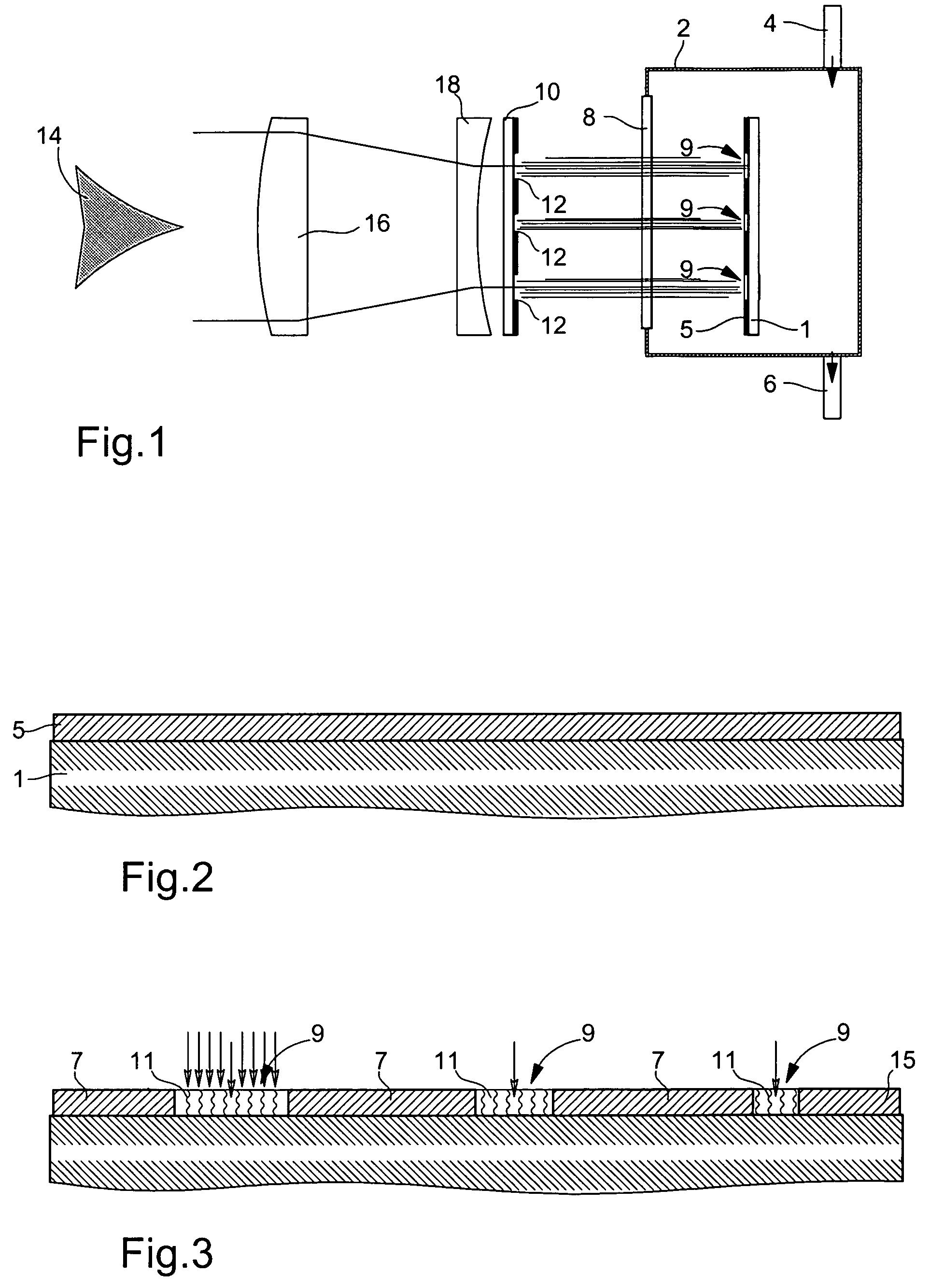
[0036]FIG. 1 shows schematically the device which basically includes a source 14 of UV radiation formed by a laser source, an optical system of the type including a convex lens 16 and a diverging lens 18 for reducing the section of the laser beam in order to increase its fluence, a mask 10 including UV radiation transparent zones 12, and an enclosed space 2. Enclosed space 2 includes a window 8 transparent to UV radiation, a gas inlet 4 and a pump outlet 6. Enclosed space 2 can also include an additional inlet (not shown) for a vector gas of a precursor gas. Inside enclosed space 2 is placed a substrate which, in this example, includes a transparent base which is already coated with a TCO film 5. It would of course be possible to form the TCO film directly in enclosed space 2, for example by LICVD, but less interesting economically, given that the energy consumption would be 100 times greater.

[0037]The UV radiation source is formed by an excimer laser, such as an XeF laser (308 nm) ...


PUM

PropertyMeasurementUnit
widthaaaaaaaaaa
thicknessaaaaaaaaaa
thicknessaaaaaaaaaa

Abstract

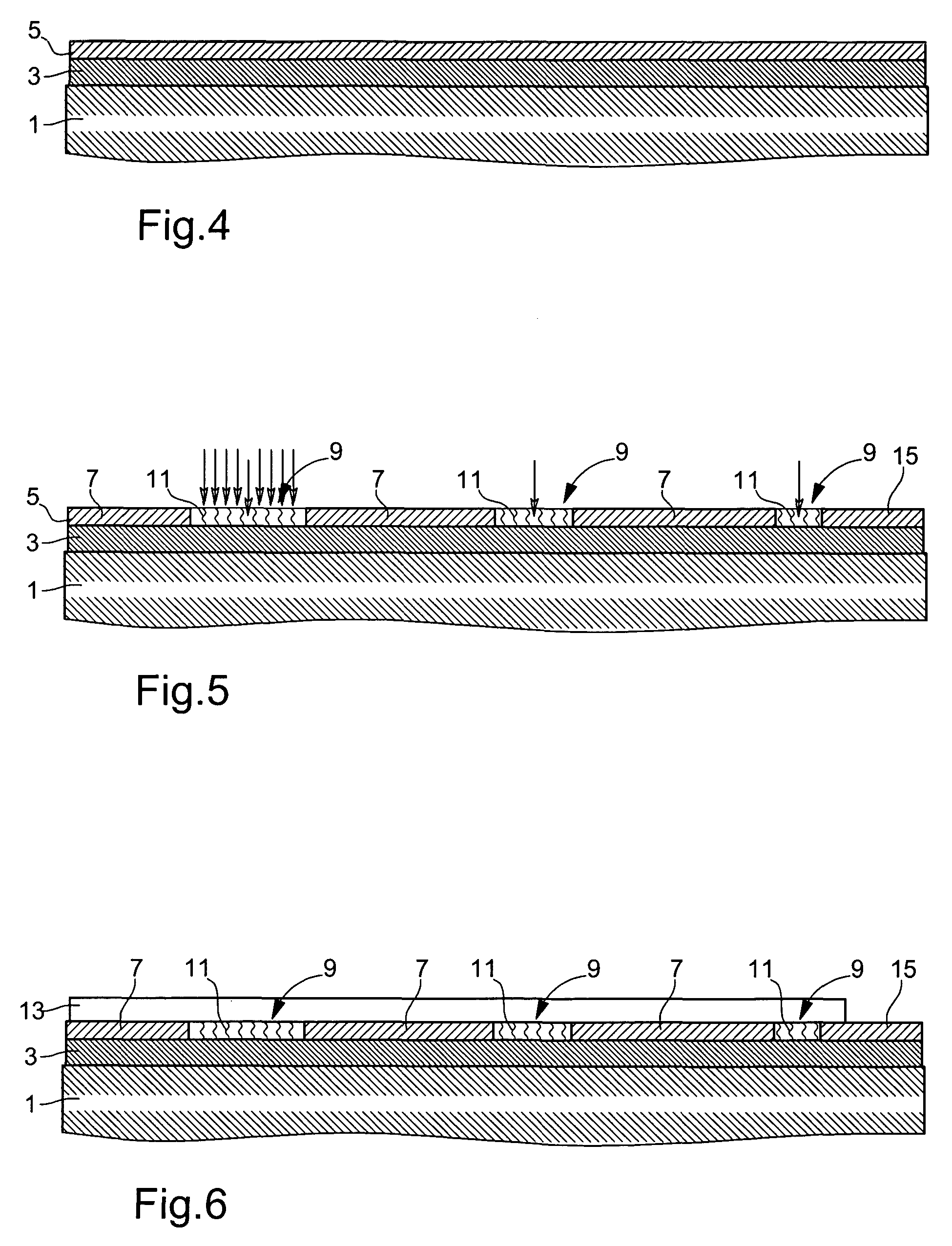
The electrodes (7) and the contact zones (15) are structured in a film of a transparent conductive oxide (TCO), deposited on a transparent support (1) possibly coated with an intermediate film (3), while being separated by dielectric spaces (9) formed by nano fissures (11) obtained by UV radiation and passing through the TCO film. A protective film (13) can coat the electrodes (7) and the dielectric spaces (9).

Description

[0001]This application claims priority from European Patent Application No. 03027566.3 filed Dec. 1, 2003, the entire disclosure of which is incorporated herein by reference.FIELD OF THE INVENTION[0002]The present invention concerns a transparent substrate having at least one face provided with transparent electrodes, whose structure is such that their contours cannot be perceived by an observer in the visible light wavelength range.[0003]The invention also concerns devices, generally electronic apparatus, including one or more transparent substrates with invisible electrodes in which the electrodes have command or electric energy collector roles, and more specifically such devices arranged above the display of an electronic apparatus on which one should be able to read the data from said display, without being disturbed by the structure and arrangement of the electrodes.[0004]The invention also concerns a method for structuring, in an economical manner and with high precision, elec...

Claims


Application Information

Patent Timeline
Patent Type & Authority Patents(United States)
IPC IPC(8): H01L31/042H01L31/0224G02F1/1343G06F3/033G06F3/041G09F9/30
CPCG02F1/13439G06F3/041Y02E10/52H01L2924/0002Y10S977/781Y10S977/784H01L2924/00Y02E10/50H01B5/14H01L31/04
Inventor POLI, GIAN-CARLOGRUPP, JOACHIMBARONI, PIERRE-YVES
Owner THE SWATCH GRP RES & DEVELONMENT LTD
Why Eureka
Eureka Blog
Learn More