Method of controlling process parameters for semiconductor manufacturing apparatus

a manufacturing apparatus and process parameter technology, applied in the field of microelectronic fabrication, can solve the problems of requiring a certain amount of non-value-added process time overhead, a significant amount of cumulative non-value added stability time, and a significant amount of cumulative overhead for a given process, so as to reduce response times, reduce the effect of stability time and reduced response tim

Inactive Publication Date: 2010-12-07
APPLIED MATERIALS INC
View PDF9 Cites 7 Cited by
  • Summary
  • Abstract
  • Description
  • Claims
  • Application Information

AI Technical Summary

Benefits of technology

[0010]Methods and systems for adaptively controlling process parameters within a process recipe executed by semiconductor manufacturing equipment are described herein. In a certain embodiment, methods and systems employing gain scheduling for PID loop tuning across steps of a process recipe may advantageously provide reduced response times where the size of the change in a process parameter setpoint between steps of a process recipe spans a wide range. Reductions in response times may enable a process recipe to have shorter stabilization times and so the methods and systems described herein are well suited for reducing the overhead associated with stabilization steps typically found between value-added manufacturing steps in a process recipe.
[0012]In a further embodiment, only the proportional gain value of the second set of PID values is different than that of the first set of PID values, with the integral and derivative values remaining constant. In one such embodiment, the proportional gain value decreases as a function of the first setpoint but increases as a function of the delta between the first and second setpoints to improve the control response across a wide range of setpoint deltas between recipe steps.

Problems solved by technology

However, each value-added step typically requires a certain amount of non-value-added process time overhead including such things as substrate handling and stability steps.
However, such in-situ recipes still typically require a stability step of a finite duration to allow the manufacturing process parameters to be switched from a setpoint used in a first value-added operation to another parameter setpoint for a subsequent value-added operation.
Depending on the duration of each stability step, the cumulative overhead for a given process may become a significant fraction of the total process time for a substrate or workpiece in a single-substrate manufacturing tool.
As evident from the graph in FIG. 1, the cumulative non-value added stability time represents a significant amount of overhead to the total process recipe time.
As the setpoint range gets wider, non-linearity in the system renders the conventional linear PID control algorithm inadequate and the response time for the extremes in the setpoint range become intolerable.

Method used


Image

  • Method of controlling process parameters for semiconductor manufacturing apparatus
  • Method of controlling process parameters for semiconductor manufacturing apparatus
  • Method of controlling process parameters for semiconductor manufacturing apparatus

Examples


Embodiment Construction

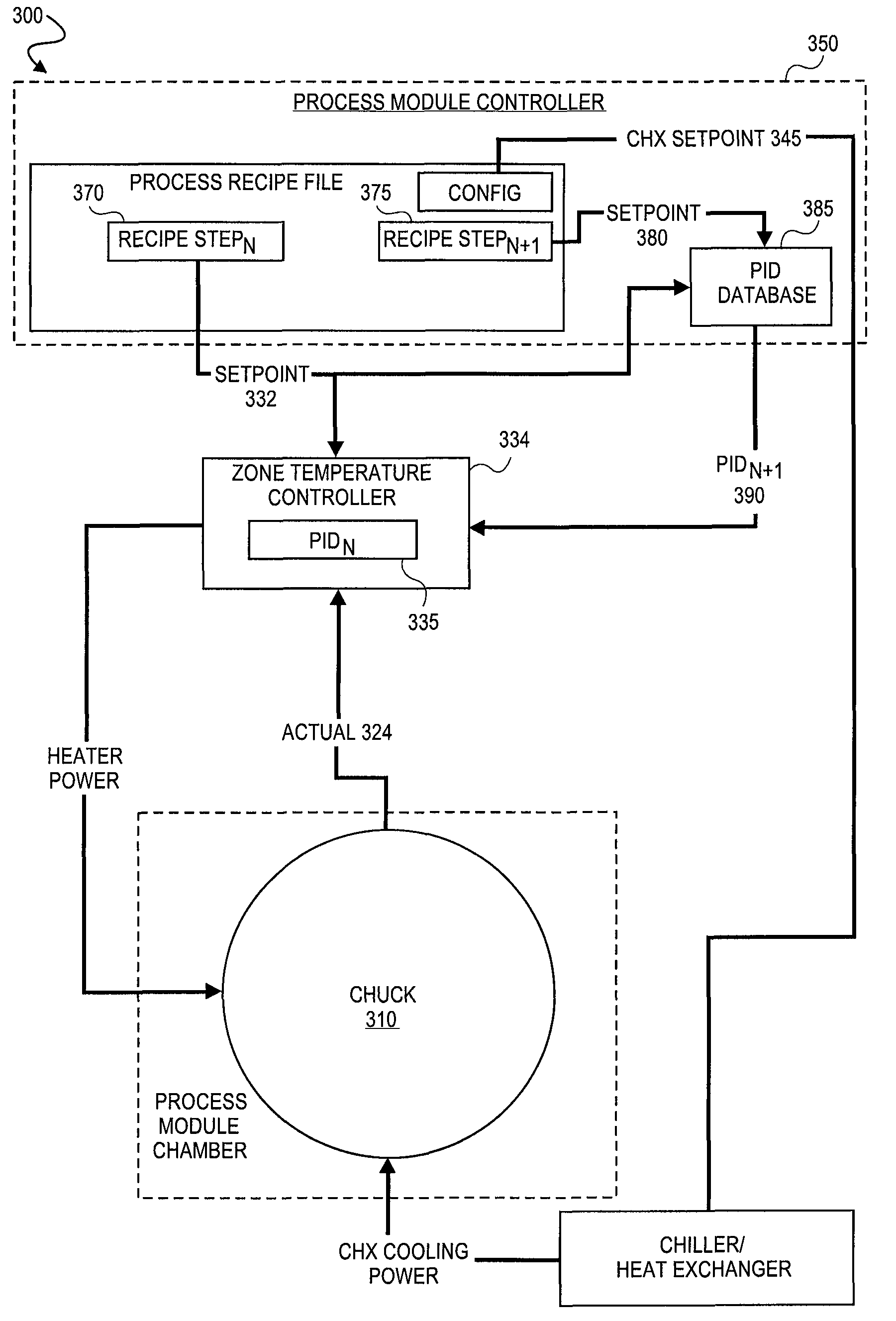
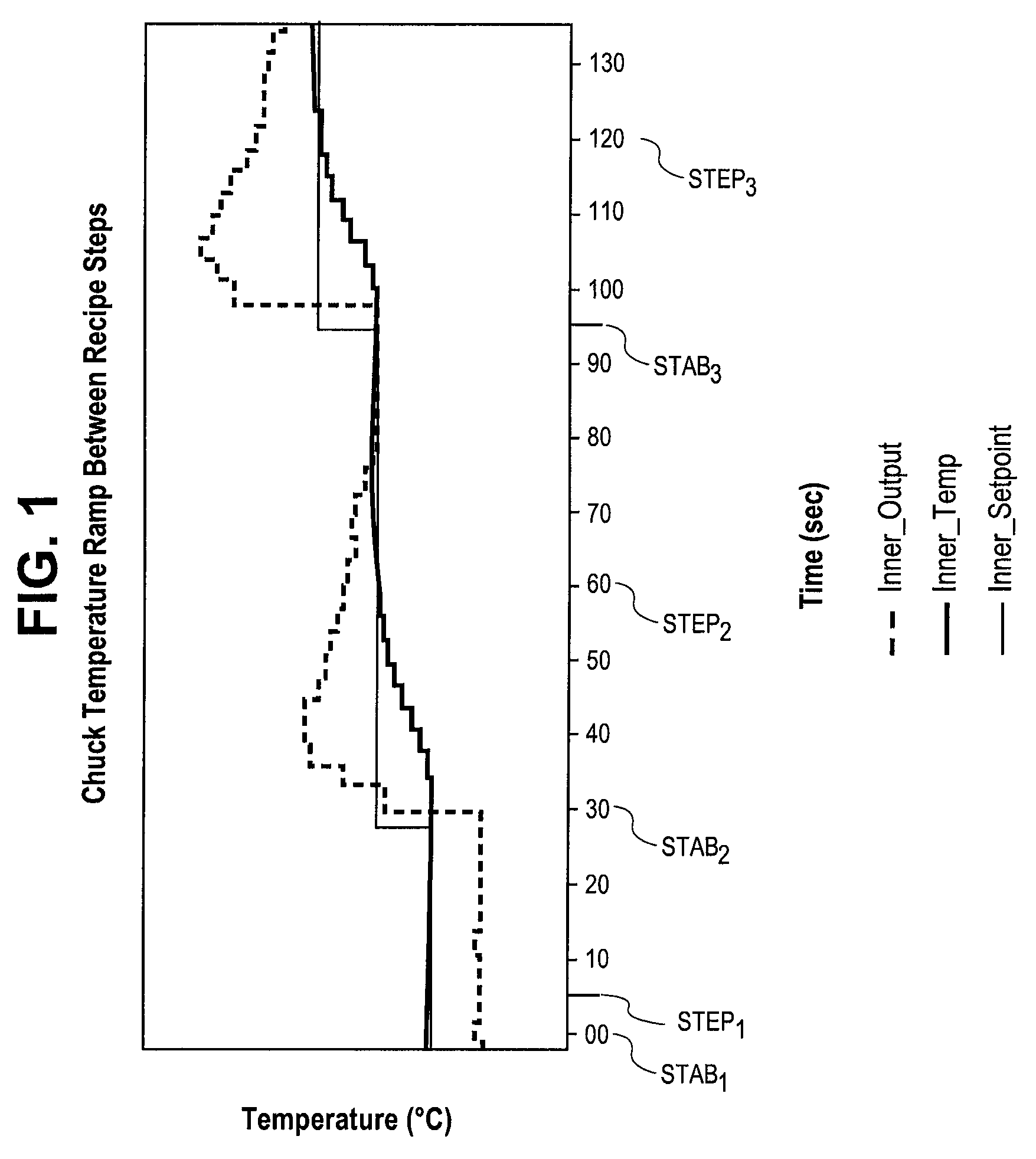
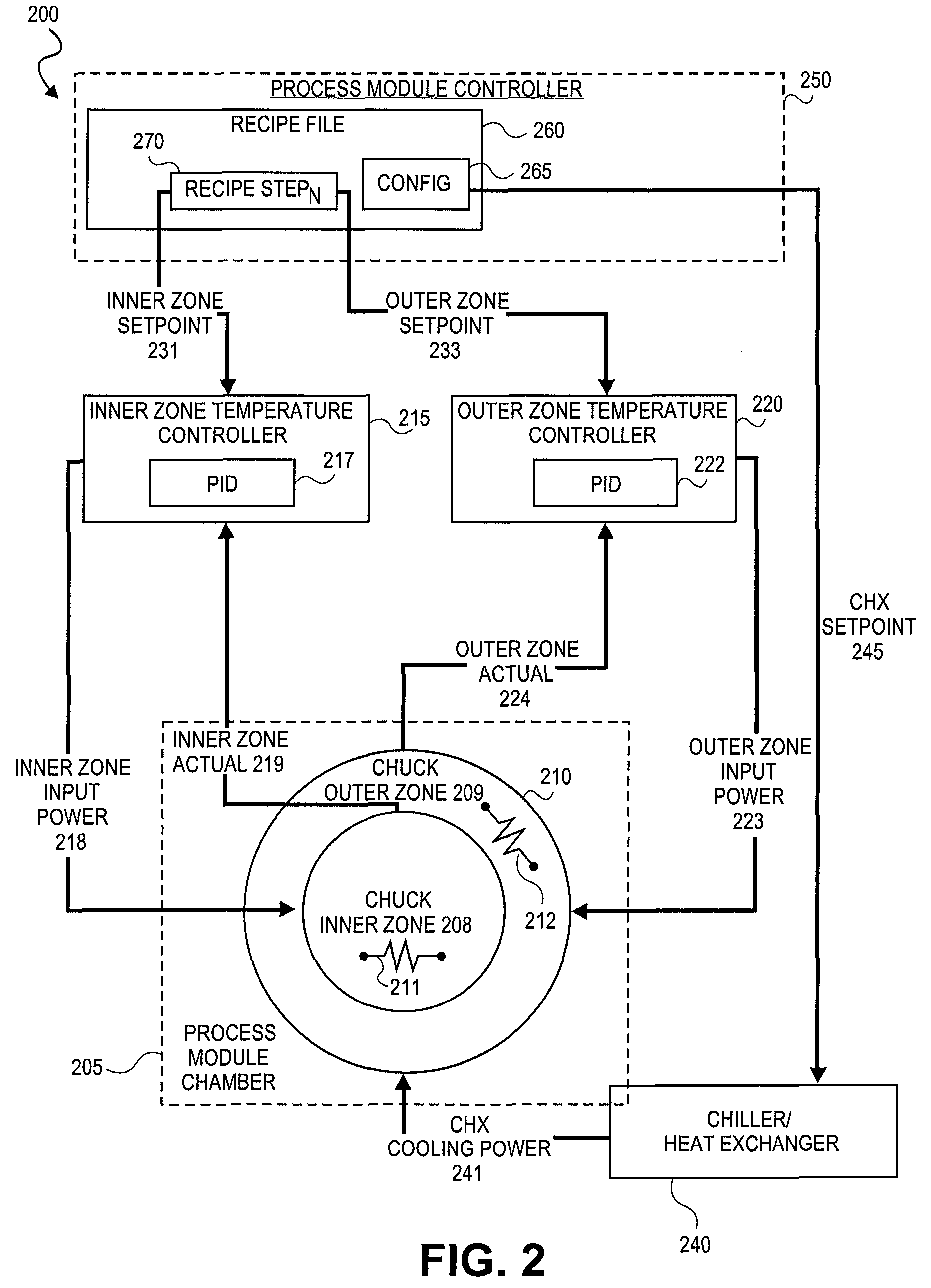
[0028]In the following description, numerous specific details are set forth, such as temperature ranges and PID gain values, to provide a thorough understanding of the present invention. It will be apparent to one skilled in the art that the present invention may be practiced without these specific details. In other instances, well-known features, such as temperature controller PID value learning techniques, are not described in detail to not unnecessarily obscure the present invention. Reference throughout this specification to “an embodiment” means that a particular feature, structure, material, or characteristic described in connection with the embodiment is included in at least one embodiment of the invention. Thus, the appearances of the phrase “in an embodiment” in various places throughout this specification are not necessarily referring to the same embodiment of the invention. Furthermore, the particular features, structures, materials, or characteristics may be combined in ...


PUM

PropertyMeasurementUnit
temperatureaaaaaaaaaa

Abstract

Methods and systems for adaptively controlling process parameters in semiconductor manufacturing equipment. An embodiment provides for gain scheduling of PID controllers across recipe steps. One embodiment provides a method for controlling a chuck temperature during a semiconductor manufacturing process, the method employing a first set of proportional-integral-derivative (PID) values in a PID controller to control the chuck temperature at a first setpoint in a first step of a process recipe and employing a second set of PID values in the PID controller to control the chuck temperature at a second setpoint, different than the first setpoint, in a second step of the process recipe. The methods and systems provide reduced controller response times where process parameter setpoint between steps of a process recipe span a wide range.

Description

CROSS REFERENCE TO RELATED APPLICATIONS[0001]This application claims the benefit of U.S. Provisional Application No. 61 / 019,188, filed Jan. 4, 2008, the entire contents of which are hereby incorporated by reference herein.BACKGROUND[0002]1) Field[0003]Embodiments of the present invention generally relate to microelectronic fabrication, and more particularly to methods of controlling a process parameter in a process recipe performed by a semiconductor manufacturing apparatus.[0004]2) Description of Related Art[0005]Today, the majority of semiconductor fabrication processes are performed with single-substrate manufacturing equipment. Improved process uniformity and control has generally outweighed the throughput reduction associated with such serial processing as compared to parallel processing of batch equipment. With the continuing reduction in the dimensions and film thicknesses formed in a given manufacturing process, the duration of each particular value-added step, such as an et...

Claims


Application Information

Patent Timeline
Patent Type & Authority Patents(United States)
IPC IPC(8): G06F19/00G05D23/00G05B11/42G05B13/00
CPCG05B11/42G05D23/1904H01L21/67098H01L21/67248
Inventor DAO, RITCHIEBRODIE, DEREKOLSZEWSKI, SCOTTNGUYEN, DUY DZHANG, CHUNLEI
Owner APPLIED MATERIALS INC
Why Eureka
Try Eureka