Test method

a test method and substrate technology, applied in the direction of material analysis using wave/particle radiation, x/gamma/cosmic radiation measurement, instruments, etc., can solve the problems of foreign material with a diameter of 20 m or more, the surface of an and the opposite substrate is likely to be damaged. , to achieve the effect of effective and rapid test of the substra

Inactive Publication Date: 2010-12-14
TOPPAN PRINTING CO LTD
View PDF16 Cites 9 Cited by
  • Summary
  • Abstract
  • Description
  • Claims
  • Application Information

AI Technical Summary

Benefits of technology

[0019]The invention has been made in order to solve the above-mentioned problems, and an object of the invention is to provide a method of testing the size and conductivity of a foreign material adhered to a substrate. A test object may be two piece of substrate sandwiching a liquid crystal for a liquid crystal display device. In particular, an object of the invention is to provide a method of effectively testing a substrate during a substrate manufacturing process.

Problems solved by technology

Nonetheless, a fine foreign material is likely to be adhered to the substrate during any one of the complicated manufacturing processes.
The foreign material adhered to the substrate is likely to damage the surface of an opposite substrate when the liquid crystal display device is assembled.
However, it has been known that, among the foreign materials, a foreign material with a diameter of 30 μm or more damages the opposite substrate.
In addition, a foreign material with a diameter of 20 μm or more is also likely to damage the opposite substrate depending on the kind of liquid crystal display devices manufactured.
When a substrate having the conductive foreign material adhered thereto is used to assemble the liquid crystal display device, the electrodes of two substrates opposite to each other are short-circuited, making it difficult to normally display an image on the screen.
If the substrate having a foreign material with a small diameter adhered thereto is excluded without discriminating conductive and non-conductive materials, non-defective substrates are also excluded, which results in a significant reduction in yield.
If the substrate having a foreign material with a small diameter adhered thereto is used during the liquid crystal display device assembly process without discriminating conductive and non-conductive materials, the assembled liquid crystal display device becomes a defective product, which results in an increase in loss.
However, it is very difficult to test whether the fine foreign material is a conductive material.
It is considered that the conductive foreign material is also caused by dust in the atmosphere of the clean room.
Therefore, the surface of the conductive foreign material is likely to be oxidized.
In the liquid crystal display device assembly process, it is assumed that the oxide film on the surface of the foreign material is damaged and a conductive inner part is exposed, which causes a short circuit.
Therefore, it is difficult to test whether there is a foreign material during a substrate manufacturing process before the liquid crystal display device assembly process.
If it takes a long time to perform the test, the test process becomes a rate-controlling process, and the overall substrate manufacturing process is delayed significantly.
However, it is impossible to test whether there is a conductive foreign material using this method.
However, in this method, the entire short-circuited liquid crystal display device is treated as a defective product.

Method used


Image

  • Test method
  • Test method
  • Test method

Examples


examples

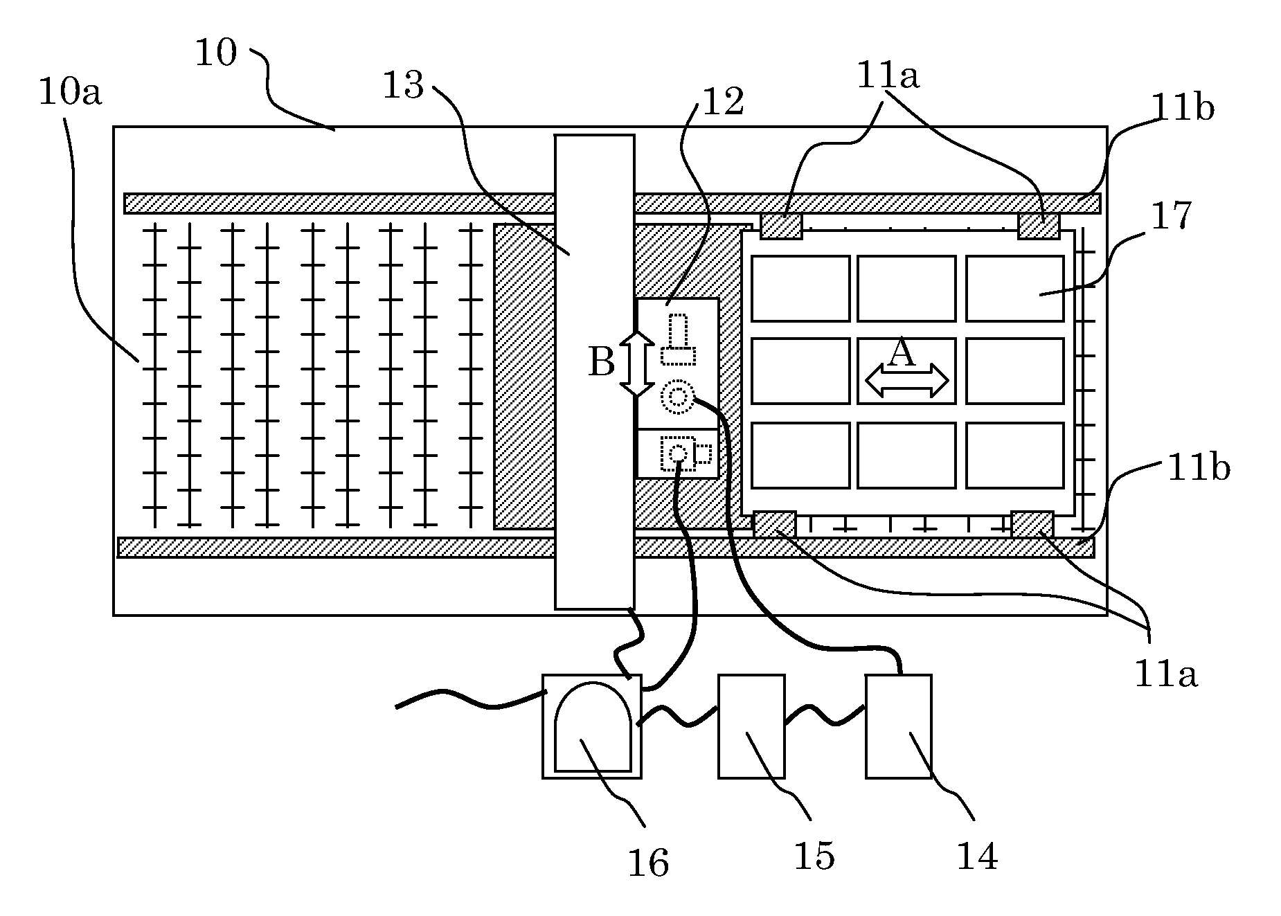
[0114]In the test device having the above-mentioned structure shown in FIG. 1, a color filter was used as a test target and the X-ray source was driven under the conditions of a tube voltage of 100 kV and a tube current of 100 mA to perform a test for a measurement time of 10 seconds. An output of 15,000 cps was obtained from an Fe particle with a diameter of about 10 μm with energy of Fe-Kα rays (cps is a unit indicating the number of X-ray photons measured per second). Under the same conditions, an output of 200 cps was obtained from a resin sphere with a diameter of about 50 μm. Under the same conditions, an output of 180 cps was obtained from a position on the color filter where there was no defect. Then, when a threshold value was set to 1,000 cps, the determining unit could detect and determine the Fe particle with a diameter of about 10 μm.


PUM

PropertyMeasurementUnit
diameteraaaaaaaaaa
diameteraaaaaaaaaa
diameteraaaaaaaaaa

Abstract

To provide a method and device for testing the size and conductivity of a foreign material adhered to a substrate for a liquid crystal display device, there is provided a method of testing whether a foreign material including a metal element is adhered to a substrate for a liquid crystal display device, the method including a first test step of detecting the size and position of the foreign material adhered to the substrate and a second test step of testing whether the foreign material includes the metal element at the position detected in the first test step.

Description

[0001]This application is a continuation of International Application No. PCT / JP2008 / 052560, filed Feb. 15, 2008, which is incorporated herein by reference in its entirety.TECHNICAL FIELD[0002]The present invention relates to a method and device for testing a fine foreign material adhered to a substrate used for a liquid crystal display device before the liquid crystal display device is assembled.BACKGROUND ART[0003]As is well known in the related art, a liquid crystal display device includes two substrates and liquid crystal sealed therebetween. In the liquid crystal display device, a voltage is applied between electrodes provided on the two substrates to drive the liquid crystal in each pixel, thereby changing the optical property of the liquid crystal. In this way, the liquid crystal display device controls the transmission and shielding of light to display an image on a screen.[0004]In general, a substrate having a glass plate as a base and liquid crystal driving electrodes prov...

Claims


Application Information

Patent Timeline
Patent Type & Authority Patents(United States)
IPC IPC(8): G01N23/223
CPCG01N23/223G01N21/94G01N2223/076
Inventor SAITO, JUNICHIHAILONG, CUI
Owner TOPPAN PRINTING CO LTD
Why Eureka
Try Eureka