Method for manufacturing a substrate with cavity

a manufacturing method and semiconductor technology, applied in printed circuit manufacturing, resist details, patterning and lithography, etc., can solve the problems of difficult to increase the mounting in the lower package, the structure of the conventional ball grip array semiconductor package is too thick to be stacked as a highly integrated memory module within a limited portion, and the package thickness is minimized. , to achieve the effect of reducing the thickness of the packag

Inactive Publication Date: 2010-12-28
SAMSUNG ELECTRO MECHANICS CO LTD
View PDF10 Cites 7 Cited by
  • Summary
  • Abstract
  • Description
  • Claims
  • Application Information

AI Technical Summary

Benefits of technology

[0010]The present invention provides a method for manufacturing a substrate with a cavity that can reduce the thickness of a package in which an integrated circuit (IC) is mounted.
[0012]Moreover, the present invention provides a method for manufacturing a substrate with a cavity that can reduce the thickness of the substrate for a package on package having three or more layers.
[0013]In addition, the present invention provides a method for manufacturing a substrate with a cavity that can reduce the total thickness of the substrate while the thickness of an insulation layer remains the same, by forming the insulation layer on sides of an external circuit.

Problems solved by technology

However, minimizing the thickness of the package has been a challenge to overcome for successful implementation of the POP technology.
This structure of a conventional ball grip array semiconductor package is too thick to be stacked as a highly integrated memory module within a limited portion.
With the conventional method, it is difficult to increase the mounting in the lower package 110 while maintaining the total thickness of the package on package.
The die-thinning method, which reduces the thickness of a semiconductor chip, can be one way of reducing the thickness, but this raises the issue of function-error with a prolonged operation.

Method used


Image

  • Method for manufacturing a substrate with cavity
  • Method for manufacturing a substrate with cavity
  • Method for manufacturing a substrate with cavity

Examples


Embodiment Construction

[0027]Hereinafter, embodiments of the invention will be described in more detail with reference to the accompanying drawings. In the description with reference to the accompanying drawings, those components are rendered the same reference number that are the same or are in correspondence regardless of the figure number, and redundant explanations are omitted.

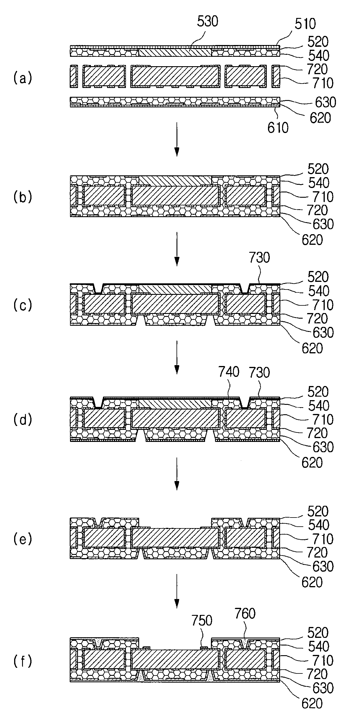
[0028]In addition, prior to describing embodiments of the present invention, a method for manufacturing a general substrate will be described first. Although a method for manufacturing a multi-layer substrate is described below, the present invention is by no means restricted to the following method for manufacturing a multi-layer substrate.

[0029]First, an internal circuit pattern is formed on the outside of a core layer. An inner-layer base material that meets the product specification is cut, and a predetermined internal circuit pattern is formed using a dry film and a working film. Here, the inner layer can be scrubbed, and a...


PUM


Abstract

An aspect of the present invention features a method for manufacturing a substrate having a cavity. The method can comprises: (a) forming an upper layer circuit on an upper seed layer; (b) laminating a dry film on a portion of the upper seed layer where a cavity is to be formed; (c) fabricating an upper outer layer by forming an insulation layer on top of the upper seed layer and on top and sides of the upper layer circuit; (d) stacking the upper outer layer on one side of a core layer where an internal circuit is formed; (e) removing the upper seed layer; and (f) forming the cavity by removing the dry film. The method for manufacturing a substrate with a cavity according to the present invention can reduce the total thickness of the substrate while the thickness of an insulation layer remains the same, by forming the insulation layer on sides of an external circuit.

Description

CROSS-REFERENCE TO RELATED APPLICATIONS[0001]This application claims the benefit of Korean Patent Application No. 10-2006-0014918 filed with the Korean Intellectual Property Office on Feb. 16, 2006, the disclosures of which are incorporated herein by reference in their entirety.BACKGROUND[0002]1. Technical Field[0003]The present invention relates to a stacked-type semiconductor packaging module, more specifically to a method for manufacturing a substrate, on which a cavity is formed.[0004]2. Description of the Related Art[0005]With the development of the electronics industry, there has been increasing demands for electronic parts that perform better and are smaller. To accommodate these demands, the semiconductor packing technologies have been evolving from packing one integrated circuit on one substrate to packing several integrated circuits on one substrate. Moreover, to address the need for realizing high-performance, high-density packages, and to meet the demand for these packag...

Claims


Application Information

Patent Timeline
Patent Type & Authority Patents(United States)
IPC IPC(8): H01L21/44
CPCH01L21/481H01L25/105H01L25/50H05K3/4658H05K3/4697H01L23/13H01L2224/16H01L2224/32145H01L2224/32225H01L2224/48091H01L2224/48227H01L2224/73265H01L2225/0651H01L2225/06568H01L2924/01078H01L2924/01079H01L2924/15153H01L2924/1517H01L2924/15311H01L2924/15331H05K1/183H05K3/205H05K2203/0568H05K2203/0571H05K2203/308H01L2924/00014H01L2924/01019H01L2225/1058H01L2924/00H01L2924/00012H01L24/73H01L2924/14H05K3/02H01L23/15
Inventor JUNG, HOE-KUKANG, MYUNG-SAMKIM, JI-EUNPARK, JUNG-HYUN
Owner SAMSUNG ELECTRO MECHANICS CO LTD
Why Eureka
Try Eureka