Optical designs for high-efficacy white-light emitting diodes

Inactive Publication Date: 2011-01-11
RGT UNIV OF CALIFORNIA
View PDF26 Cites 60 Cited by
  • Summary
  • Abstract
  • Description
  • Claims
  • Application Information

AI Technical Summary

Benefits of technology

[0021]The WLED may comprise more than one optically functional interface, for example, two (or more) optically functional interfaces. The optically functional interface may be positioned at a distance from the LED at least equal to a lateral extent of the LED. The optically functional interface may comprise a first material. The optically functional interface may comprise a surface of the first material and the material may be positioned such that its refractive index increases total internal reflection of the secondary light inside the secondary emitting species at the optically functional interface.
[0022]The secondary emitting species may be a phosphor layer emitting the secondary light when optically pumped by the primary light, the second material may at least partially surround the LED and be positioned such that the second material's refractive index reduces the primary light's total internal reflection inside the LED at an interface between the LED and the second material; and the first material may be positioned between the secondary emitting species and the second material.
[0031]The LED may be an LED die and the secondary emitting species may be a phosphor layer, and the method may further comprise encapsulating the LED die with a first material and a header or LED cup, wherein the first material comprises a dome shaped outer surface and is positioned such that the first material's refractive index reduces the primary light's total internal reflection inside the LED at an interface between the LED and the first material; and capping the outer surface with the one or more optically functional interfaces comprising a second material, wherein the second material has a refractive index smaller than the phosphor layer's refractive index and the one or more optically functional interfaces reflect the secondary light away from the material.

Problems solved by technology

With the other remote-phosphors geometry (as shown in FIG. 3 and FIG. 4), the situation is nearly similar, and in addition another complication stems from the fact that a smooth upper interface separating the phosphors layer and air is present near the phosphors.

Method used


Image

  • Optical designs for high-efficacy white-light emitting diodes
  • Optical designs for high-efficacy white-light emitting diodes
  • Optical designs for high-efficacy white-light emitting diodes

Examples


examples

(1) Using a Commercially Available Blue LED Chip

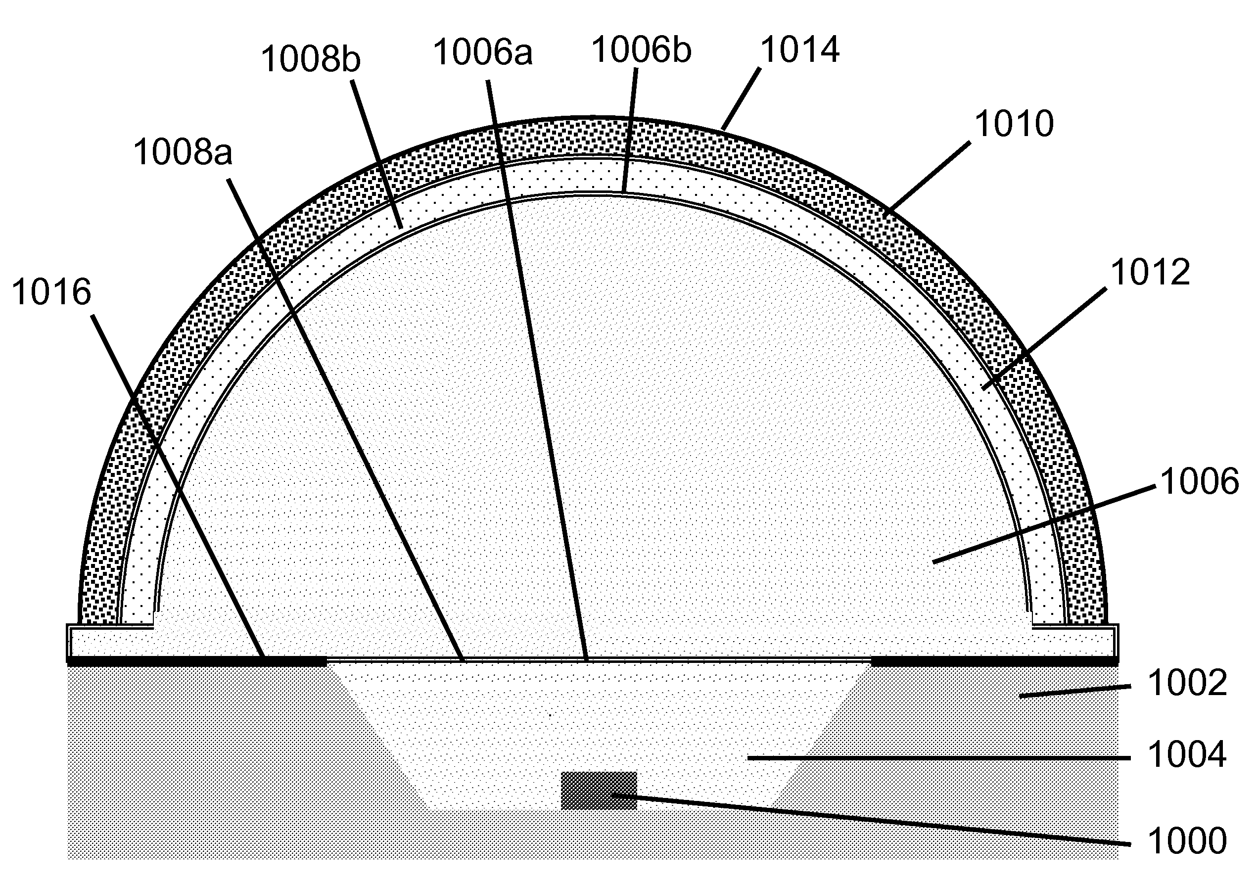
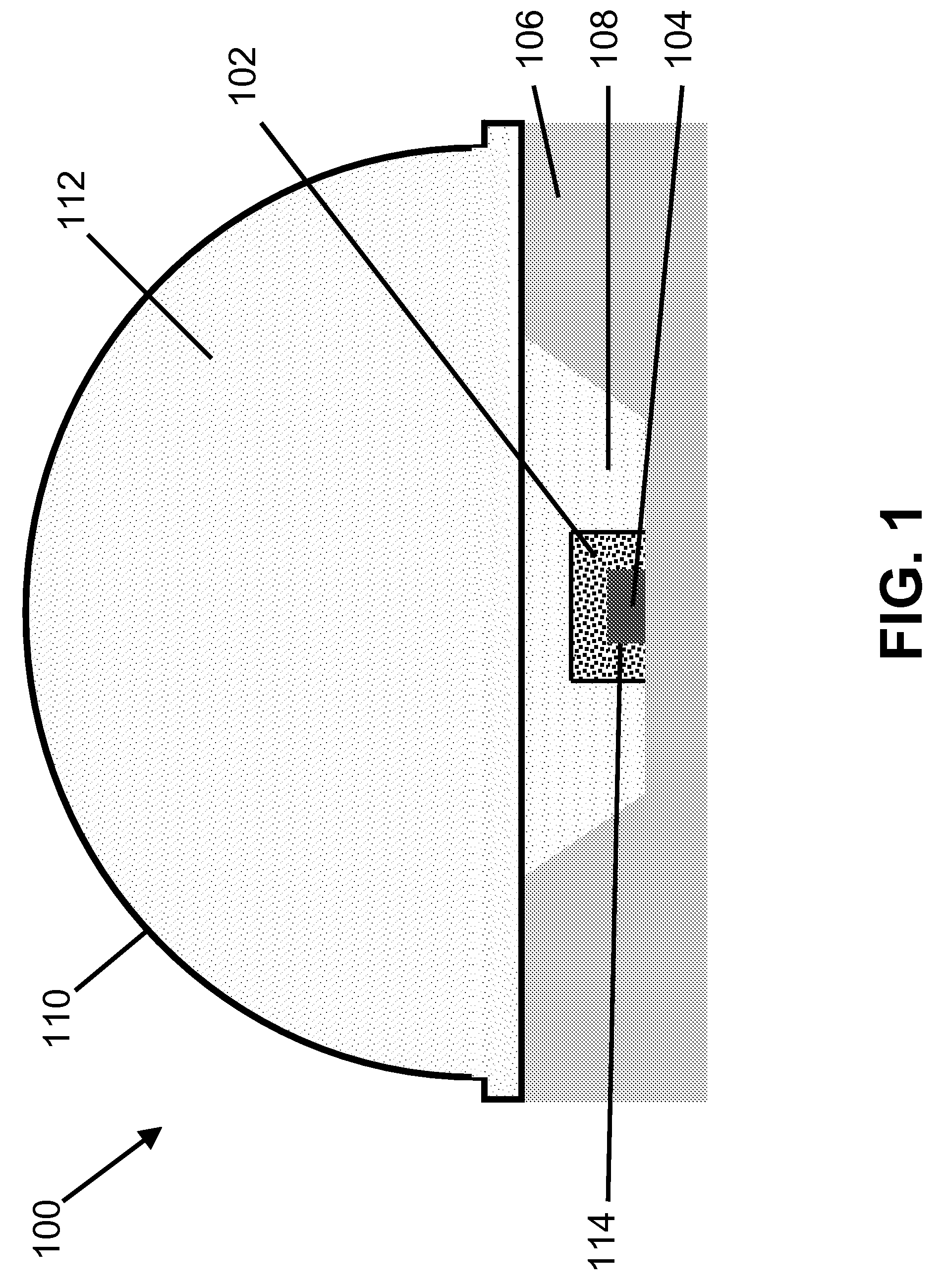
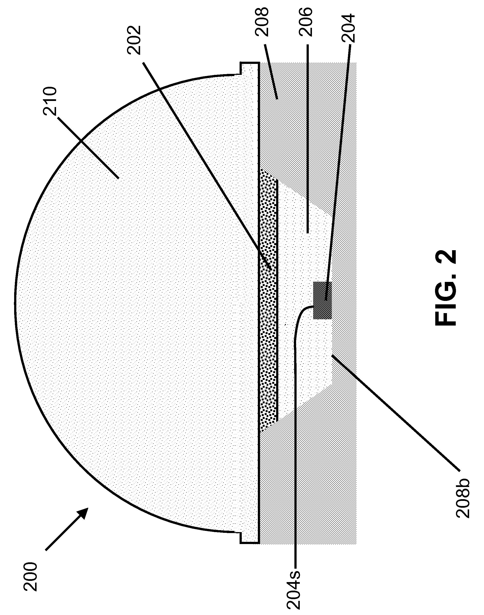
[0076]FIG. 19 shows a schematic of a device 1900. A blue LED lamp was formed by attaching a commercially-available CREE EZR450 LED die or chip 1902 onto a silver header 1904 by using silver epoxy. Silver epoxy allows for vertical electrical conduction throughout the LED die 1902; more specifically, it allows the injection of holes traveling from the silicon submount to the p-doped GaN layers and active layers including InGaN quantum wells. The top contact (n-contact) of this die 1902 was connected by a gold wire 1906 to the first (header) post 1908 of the silver header 1904 via wire-bonding. The other (second) post 1910 of the silver header 1904 was connected by another gold wire 1912 to the header 1904 itself via wire-bonding. At this stage, the total radiant flux ΦB of the bare LED die 1902 on silver header 1904 was measured using a calibrated integrating sphere to be 21.0 mW at 20 mA and 3.20 V (DC measurement). The wavelength of li...


PUM


Abstract

A method for increasing the luminous efficacy of a white light emitting diode (WLED), comprising introducing optically functional interfaces between an LED die and a phosphor, and between the phosphor and an outer medium, wherein at least one of the interfaces between the phosphor and the LED die provides a reflectance for light emitted by the phosphor away from the outer medium and a transmittance for light emitted by the LED die. Thus, a WLED may comprise a first material which surrounds an LED die, a phosphor layer, and at least one additional layer or material which is transparent for direct LED emission and reflective for the phosphor emission, placed between the phosphor layer and the first material which surrounds the LED die.

Description

CROSS-REFERENCE TO RELATED APPLICATIONS[0001]This application claims the benefit under 35 U.S.C. Section 119(e) of commonly-assigned U.S. Provisional Patent Application Ser. No. 60 / 946,652, filed on Jun. 27, 2007, by Frederic S. Diana, Steven P. DenBaars, and Shuji Nakamura, entitled “OPTICAL DESIGNS FOR HIGH-EFFICACY WHITE-LIGHT EMITTING DIODES”, which application is incorporated by reference herein.BACKGROUND OF THE INVENTION[0002]1. Field of the Invention[0003]This invention is related to semiconductor light-emitting diodes (LEDs) and in particular presents optimized optical designs aimed at improving the luminous efficacy of white-light emitting diodes (WLEDs) used for lighting applications.[0004]2. Description of the Related Art[0005]Currently, there exists a multitude of WLED packaging configurations in the state of the art. The term packaging encompasses a broad technical scope. With respect to LEDs it refers to all the fabrication steps which follow wafer processing: dicing ...

Claims


Application Information

Patent Timeline
Patent Type & Authority Patents(United States)
IPC IPC(8): H01L33/00H01L33/48H01L33/50H01L33/58
CPCH01L33/60H01L33/50H01L33/507H01L33/46H01L33/483H01L33/58H01L2224/48091H01L2224/45144F21K9/64H01L2924/19107H01L2924/00014H01L2924/00H01L33/32H01L33/504H01L33/505H01L2933/0041H01L2933/0058
Inventor DIANA, FREDERIC S.DENBAARS, STEVEN P.NAKAMURA, SHUJI
Owner RGT UNIV OF CALIFORNIA
Why Eureka
Try Eureka