
Inspection method and its apparatus, inspection system
a technology of inspection method and inspection system, applied in the field of inspection, can solve the problems of difficult to improve a yield effectively, not efficiently reviewing the necessary defect, not being taken by priority, etc., and achieve the effect of improving the efficiency of inspection
- Summary
- Abstract
- Description
- Claims
- Application Information
AI Technical Summary
Benefits of technology
Problems solved by technology
Method used
Image

Examples
Embodiment Construction
[0043]Preferred embodiments of a method for inspecting a semiconductor device and its tool, and preferred embodiments of a method for manufacturing the semiconductor device, according to the present invention, will be described below with reference to the drawing.
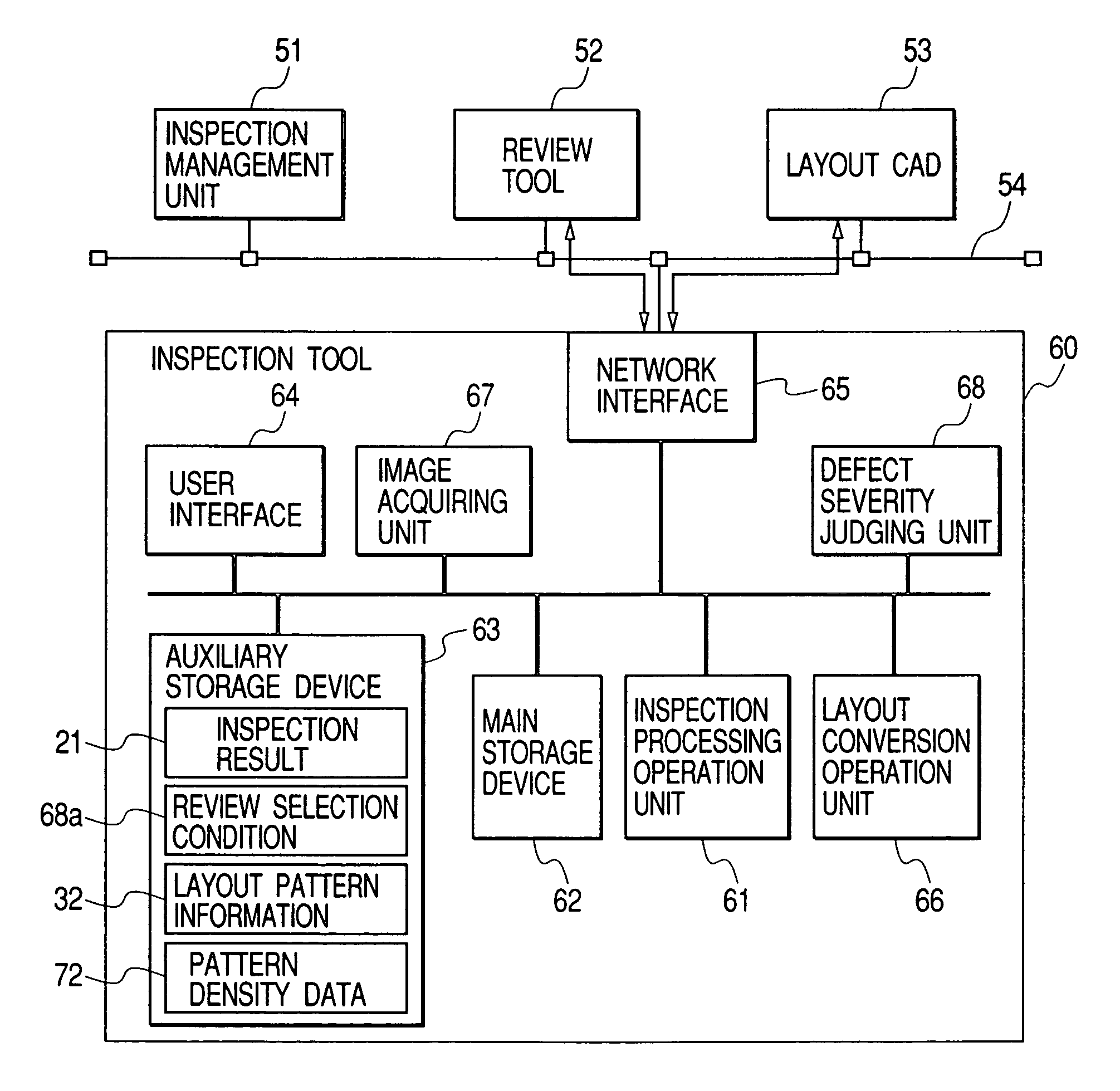
[0044]FIG. 9 illustrates a distribution map 36 showing how positions of defects detected by an inspection-processing unit 61 of an inspection tool 60 in a configuration shown in FIG. 1 are distributed in a chip. This distribution map 36 showing the defect positions distributed in the chip is made by plotting data 35 of the detected defects on a schematic diagram 32 illustrating a circuit layout of a LSI chip. To be more specific, the detected defects are plotted according to position coordinates in respective LSI chips on a wafer. Each black dot indicates an individual defect. Rectangular frames B1 through B7 indicate positions of LSI function block 1 through LSI function block 7, respectively. Here, the LSI function blocks...
PUM
| Property | Measurement | Unit |
|---|---|---|
| angle | aaaaa | aaaaa |
| size | aaaaa | aaaaa |
| defect | aaaaa | aaaaa |
Abstract
Description
Claims
Application Information