Panel and method for manufacturing the same

a technology of liquid crystal panels and sealants, applied in the field of panels, can solve the problems of uncured sealant impurities leaking into the liquid crystal layer, and achieve the effects of preventing any increase in the production cost of sealants, reducing the size of uncured portions, and ensuring the reliability of liquid crystal panels

Inactive Publication Date: 2011-02-01
SHARP KK
View PDF29 Cites 9 Cited by
  • Summary
  • Abstract
  • Description
  • Claims
  • Application Information

AI Technical Summary

Benefits of technology

[0012]In order to overcome the problems described above, preferred embodiments of the present invention provide a liquid crystal panel which prevents any increase in the production cost thereof, reduces the size of an uncured portion of a sealant, and in which components of the sealant are less likely to leak into a liquid crystal layer, so as to ultimately ensure the reliability of liquid crystal panels while maintaining excellent display quality.
[0013]According to a preferred embodiment of the present invention, a light-shielding layer having a slit that is in a negative / positive relationship with a line on a first substrate is formed immediately outside a display region of a second substrate provided with a sealant. In this way, the problems described above are solved. More specifically, a panel according to a preferred embodiment of the present invention includes a first substrate, a second substrate opposed to the first substrate, and a sealant disposed between the first substrate and the second substrate and formed between portions of the first and second substrates located immediately outside the display region. At least the portion of the first substrate located immediately outside the display region is provided with lines exhibiting a light blocking effect. On the other hand, the portion of the second substrate located immediately outside the display region is provided with a light-shielding layer, and slits are formed in regions of the light shielding layer coinciding with the lines. According to the panel of various preferred embodiments of the present invention, the sealant can be cured by applying light through both sides of the panel. This can reduce the size of an uncured portion of the sealant.
[0016]In particular, since light can be applied through both sides of the liquid crystal panel of various preferred embodiments of the present invention to the sealant, use of a photopolymerized sealant can shorten the sealant curing period and the period during which the liquid crystal layer is in contact with the uncured sealant. In view of this, in the liquid crystal panel according to preferred embodiments of the present invention, the possibility of components of the sealant leaking into the liquid crystal layer is further reduced. As a result, the display quality of the panel can be maintained with higher reliability.
[0017]The liquid crystal panel according to preferred embodiments of the present invention may further include a barrier formed inside the sealant and extending along the sealant. In this case, the surface of the barrier near the sealant may be inclined. Since this liquid crystal panel has a barrier formed inside the sealant (on the side of the sealant near the liquid crystal layer), this can prevent components of the uncured sealant from being in contact with the liquid crystal layer during the period from the bonding between the first and second substrates to the curing of the sealant. Furthermore, since the surface of the barrier near the sealant is inclined, the area of contact between the barrier and the sealant becomes larger than when the surface of the barrier near the sealant is perpendicular to the panel surface. Therefore, the reliability with which the sealant and the barrier are bonded to each other is increased. This can prevent the relative displacement between the first substrate and the second substrate with higher reliability. Furthermore, the width of the sealant can be reduced, resulting in a reduction in the size of a non-display region of the liquid crystal display panel which corresponds to an edge portion thereof and does not contribute to display. In summary, the liquid crystal display panel can be reduced in size.
[0019]According to the method of one preferred embodiment of the present invention, in the method for manufacturing a liquid crystal panel in which a one-drop fill method is used, the sealant can be sufficiently cured only by photoirradiation. This can reduce the possibility of impurities in the sealant leaking into the liquid crystal layer as compared with when a photoreactive and heat-reactive sealant is used. In view of this, the display quality of the panel can be maintained with higher reliability, thereby ensuring the reliability of the liquid crystal panel.
[0020]According to various preferred embodiments of the present invention, uncured portions of the sealant can be reduced in area. In a case where preferred embodiments of the present invention are applied to a liquid crystal panel, the possibility of components of a sealant leaking into a liquid crystal layer can be reduced while the production cost is prevented from increasing. In view of this, excellent display quality can be maintained, thereby ensuring the reliability of the liquid crystal panel.

Problems solved by technology

However, impurities in an uncured sealant may leak into the liquid crystal layer by the heating for thermal curing, and therefore a photopolymerized sealant is more preferably used as the sealant than a photoreactive and heat-reactive sealant.

Method used


Image

  • Panel and method for manufacturing the same
  • Panel and method for manufacturing the same
  • Panel and method for manufacturing the same

Examples


first preferred embodiment

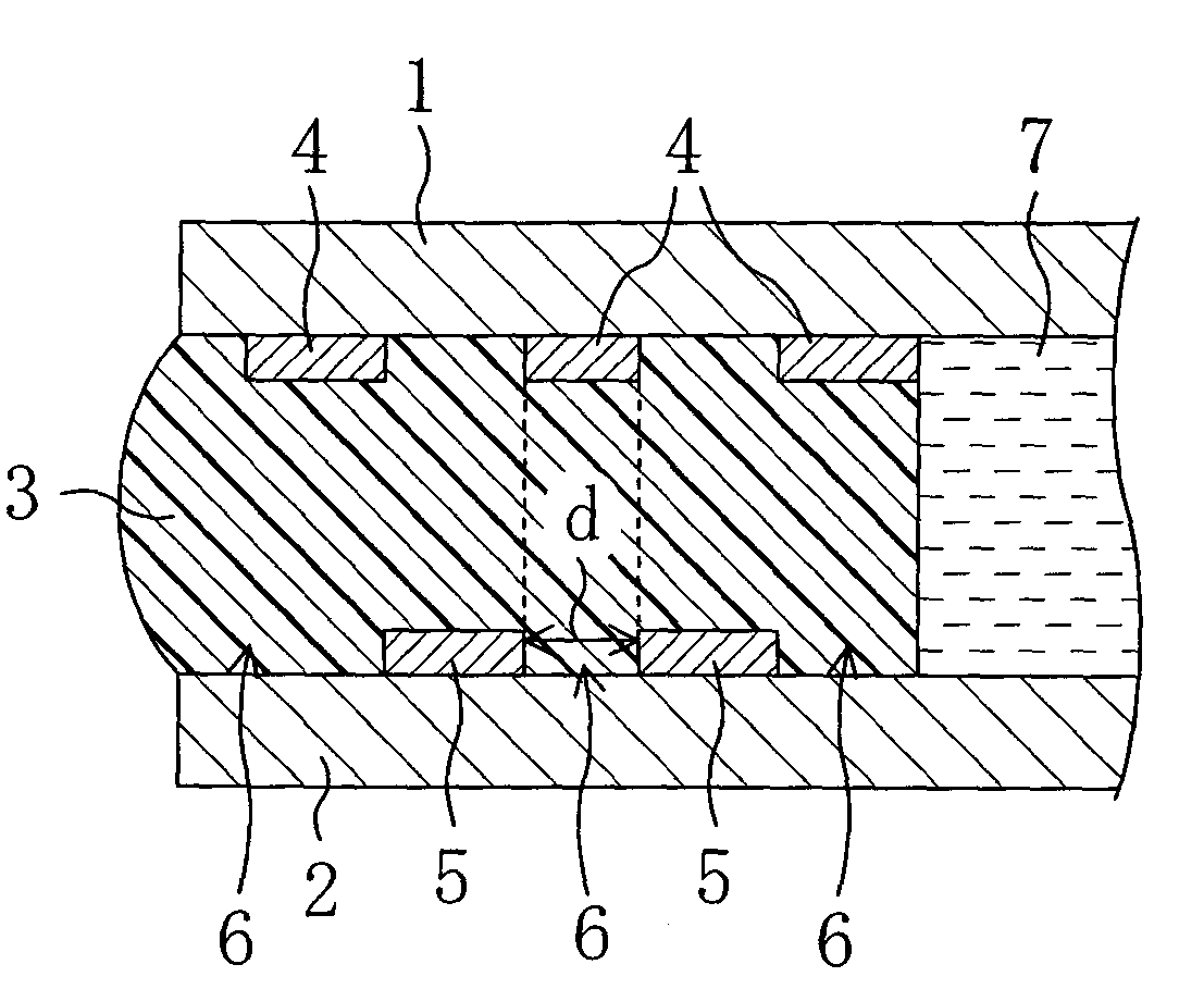
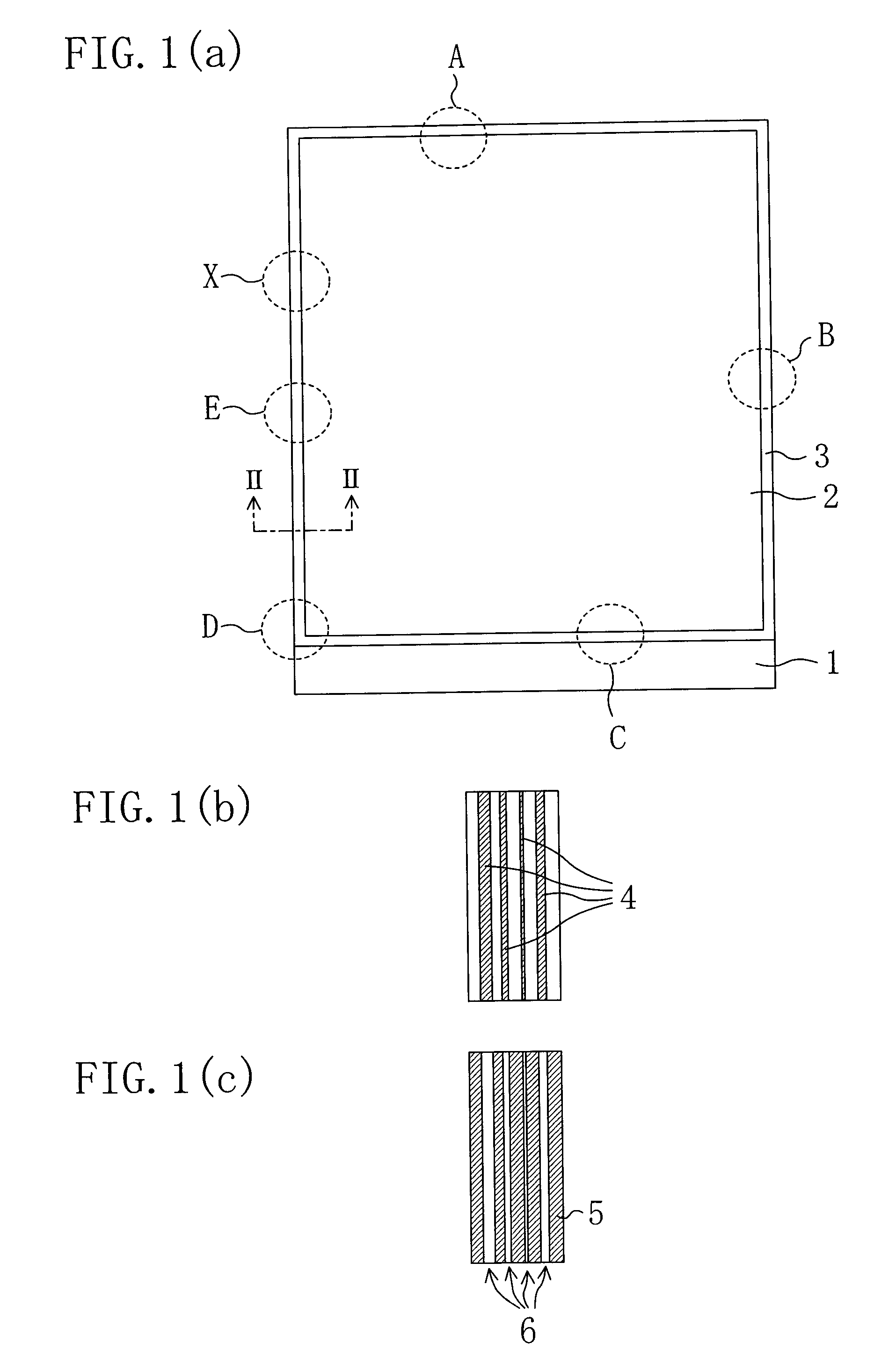
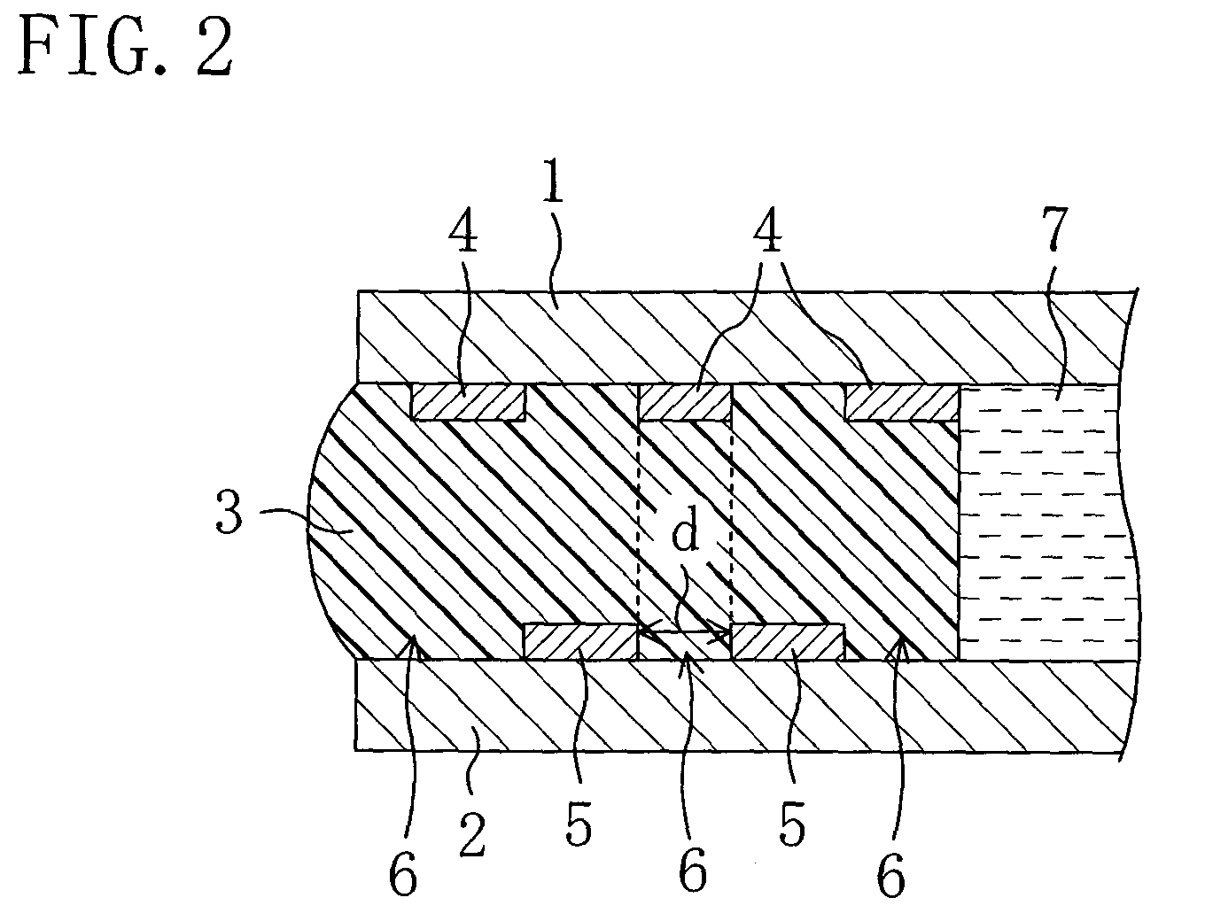
[0030]FIG. 1(a) is a plan view schematically illustrating a liquid crystal display panel according to a first preferred embodiment, FIG. 1(b) is a schematic enlarged view of a portion of a TFT substrate 1 surrounded by X in FIG. 1(a), and FIG. 1(c) is a schematic enlarged view of a portion of a color filter substrate 2 surrounded by X in FIG. 1(a). FIG. 2 is a cross-sectional view taken along the line II-II in FIG. 1(a).

[0031]The liquid crystal display panel of this preferred embodiment includes a TFT substrate 1 serving as a first substrate, a color filter (CF) substrate 2 opposed to the TFT substrate 1 and serving as a second substrate, a sealant 3 disposed between the TFT substrate 1 and the CF substrate 2 and formed between respective portions of both the substrates 1 and 2 located immediately outside display regions of the substrates 1 and 2, and a liquid crystal layer 7 disposed between the TFT substrate 1 and the CF substrate 2.

[0032]The TFT substrate 1 includes a plurality o...

second preferred embodiment

[0048]FIG. 5 is a schematic cross-sectional view of a portion of a liquid crystal display panel located in the vicinity of one end of a display region of the panel according to a second preferred embodiment. In the subsequent drawings, components having substantially the same functions as the components of the liquid crystal display panel of the first preferred embodiment are denoted by the same reference numerals, and thus description thereof will be omitted.

[0049]The liquid crystal display panel of this preferred embodiment further includes a barrier 8 continuously formed inside a loop-like sealant 3 (on the side of the sealant 3 near a liquid crystal layer 7) so as to extend along the sealant 3. The liquid crystal layer 7 is surrounded by the barrier 8.

[0050]The barrier 8 has an inclined surface 81 near the sealant 3 and a side surface 82 near the liquid crystal layer 7 and is preferably formed of an optically transparent material. For example, a photopolymerized organic material...


PUM

PropertyMeasurementUnit
widthaaaaaaaaaa
widthaaaaaaaaaa
widthaaaaaaaaaa

Abstract

A liquid crystal display panel includes a TFT substrate, a color filter (CF) substrate opposed to the TFT substrate, a sealant disposed between the TFT substrate and the CF substrate and disposed between portions of both the substrates located immediately outside display regions thereof, and a liquid crystal layer disposed between the TFT substrate and the CF substrate. The CF substrate is provided with a light-shielding layer at a portion located immediately outside its display region. The light-shielding layer is provided with a slit at a region that coincides with a line on the TFT substrate.

Description

BACKGROUND OF THE INVENTION[0001]1. Field of the Invention[0002]The present invention relates to panels and methods for manufacturing the same, and more particularly relates to liquid crystal panels formed with liquid crystal layers by a one-drop fill method.[0003]2. Description of the Related Art[0004]Process steps for manufacturing a liquid crystal panel include the process step of charging a liquid crystal material into a panel. Methods for charging a liquid crystal material into a panel include a dip method and a dispenser method. In these methods, the following technique is used: A pair of substrates are bonded to each other with a sealant interposed therebetween, then a liquid crystal material is charged through an opening of the sealant into a panel by utilizing capillarity and a differential pressure, and then the opening is sealed. However, with an increase in the screen size, the cycle time for charging a liquid crystal material into a panel is becoming longer.[0005]In rec...

Claims


Application Information

Patent Timeline
Patent Type & Authority Patents(United States)
IPC IPC(8): G02F1/1339
CPCG02F1/1339G02F1/133509G09F9/30
Inventor KONDO, MASAHIKOJOGAN, SHINGO
Owner SHARP KK
Why Eureka
Try Eureka