
Device and method for the demodulation electromagnetic wave fields having separated detection and demodulation regions

a technology of electromagnetic wave field and demodulation region, which is applied in the direction of amplifiers controlled by light, using reradiation, television systems, etc., to achieve the effects of less susceptibility, less susceptibility, and improved spatial (lateral) sampling of the scen

Active Publication Date: 2011-02-08
AMS SENSORS SINGAPORE PTE LTD
View PDF6 Cites 69 Cited by
  • Summary
  • Abstract
  • Description
  • Claims
  • Application Information

AI Technical Summary

Benefits of technology

The present invention provides a pixel device that can detect and demodulate electromagnetic waves with high sensitivity and speed. The device includes a detection system, a sampling system, and demodulation means. The detection system converts the incident electromagnetic wave field into an electric signal of flowing charges, while the sampling system samples the electric signal at different time intervals during a modulation period. The demodulation means uses a lateral, static drift field to transfer the signal of flowing charges to the output nodes, allowing for high-speed demodulation. The pixel device is advantageous in applications where high sensitivity and high-speed demodulation are required, such as three-dimensional imaging and optical data transfer. The invention also provides a design for non-stripe-like structures and efficient use of micro-lens arrays. Overall, the invention provides a pixel device with high sensitivity, speed, and adaptability for various applications.

Problems solved by technology

Furthermore, the small size of the demodulation area means small parasitic capacitances of the control gates which have to be quickly charged or recharged so that a large number of pixels can be driven with high frequencies at the same time.

Method used


Image

  • Device and method for the demodulation electromagnetic wave fields having separated detection and demodulation regions
  • Device and method for the demodulation electromagnetic wave fields having separated detection and demodulation regions
  • Device and method for the demodulation electromagnetic wave fields having separated detection and demodulation regions

Examples


Embodiment Construction

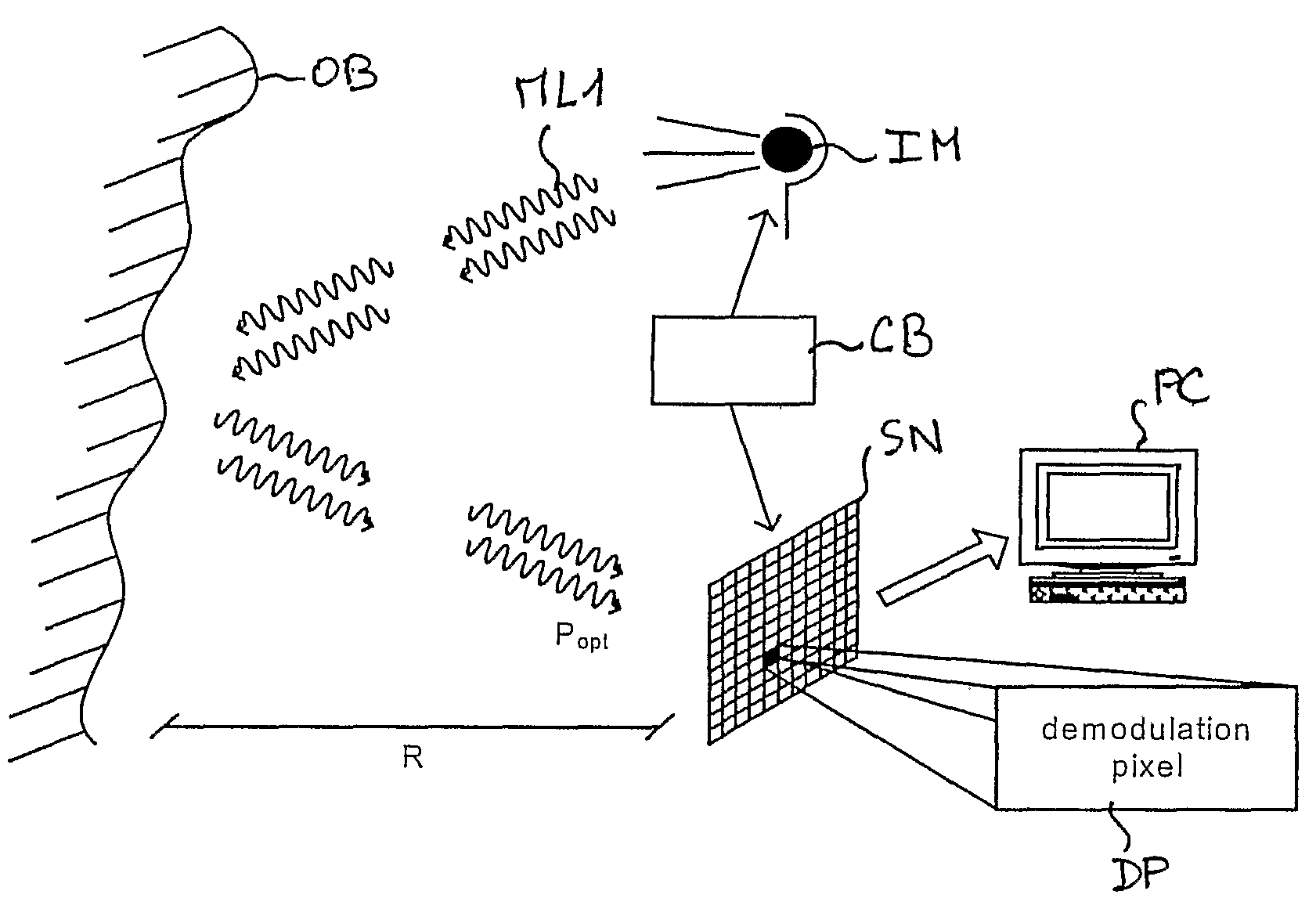
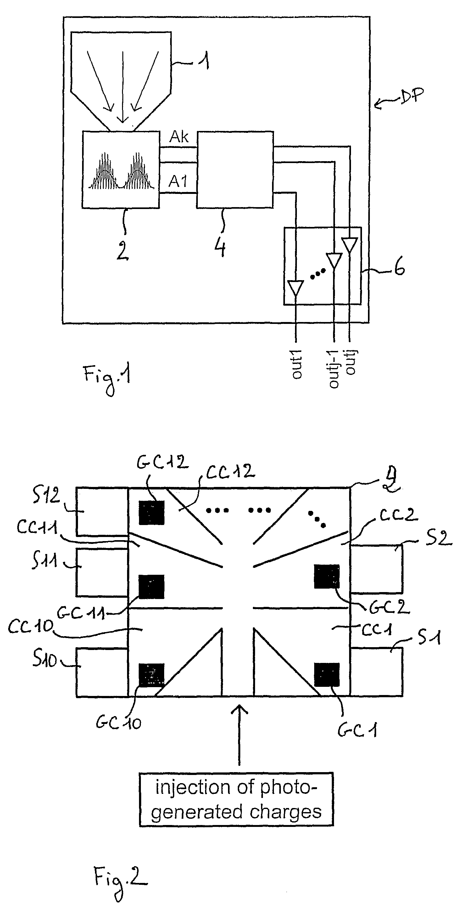
[0038]FIG. 1 shows a photo-sensitive pixel according to the invention. This photo-sensitive pixel DP comprises a photo-sensitive detection region 1, a demodulation region 2, an optional stage 4 for any kind of data processing and optionally amplification circuitry 6. On reception of electromagnetic radiation, e.g. light radiation, on the photo-sensitive area of the detection region 1 and potentially of the demodulation region 2, photo charge carriers are generated.

[0039]The detection region 1, in particular if largely designed, needs to transport the photo-generated charge carriers to the demodulation region 2 as fast as possible in order to minimize any low-pass filtering effects on the opto-electronically converted signal, also called electric signal of flowing charges or photo-current signal. The fast charge-carrier transport to the demodulation region 2 is realized by a lateral drift field into the particular direction. That drift field can be generated by various methods. The f...


PUM


Abstract

A new pixel in semiconductor technology comprises a photo-sensitive detection region (1) for converting an electromagnetic wave field into an electric signal of flowing charges, a separated demodulation region (2) with at least two output nodes (D10, D20) and means (IG10, DG10, IG20, DG20) for sampling the charge-current signal at least two different time intervals within a modulation period. A contact node (K2) links the detection region (1) to the demodulation region (2). A drift field accomplishes the transfer of the electric signal of flowing charges from the detection region to the contact node. The electric signal of flowing charges is then transferred from the contact node (K2) during each of the two time intervals to the two output nodes allocated to the respective time interval. The separation of the demodulation and the detection regions provides a pixel capable of demodulating electromagnetic wave field at high speed and with high sensitivity.

Description

FIELD OF THE INVENTION[0001]The present invention relates to a pixel device for the detection and the demodulation of modulated electromagnetic waves, in particular waves of frequencies within the optical frequency spectrum, according to the preambles of the independent claims.[0002]The pixel device can be exploited in all applications demanding high photo-sensitive pixel coupled with fast samplings on-pixel. These pixel characteristics are especially sought for demodulating temporally intensity-modulated electromagnetic light waves. Such pixels are particularly interesting for non-contact distance measuring sensors based on the time-of-flight principle or interferometry but as well as in phase-measuring bio (chemical) applications such as fluorescence applications.BACKGROUND OF THE INVENTION[0003]In the German patent DE4440613C1 (Spirig, “Vorrichtung und Verfahren zur Detektion eines intensitätsmodulierten Strahlungsfeldes”, 1996), a demodulation device is presented which samples t...

Claims


Application Information

Patent Timeline
Patent Type & Authority Patents(United States)
IPC IPC(8): H01L27/00
CPCH01L31/02005H01L27/14603G01S7/4863G01S17/89G01S17/894H04N25/77H04N25/771H04N25/772H04N5/66
Inventor BUETTGEN, BERNHARD
Owner AMS SENSORS SINGAPORE PTE LTD
Learn More