Low capacitance ESD protection structure for high speed input pins
- Summary
- Abstract
- Description
- Claims
- Application Information
AI Technical Summary
Benefits of technology
Problems solved by technology
Method used
Image

Examples
Embodiment Construction
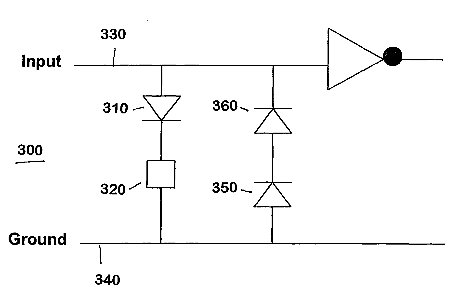
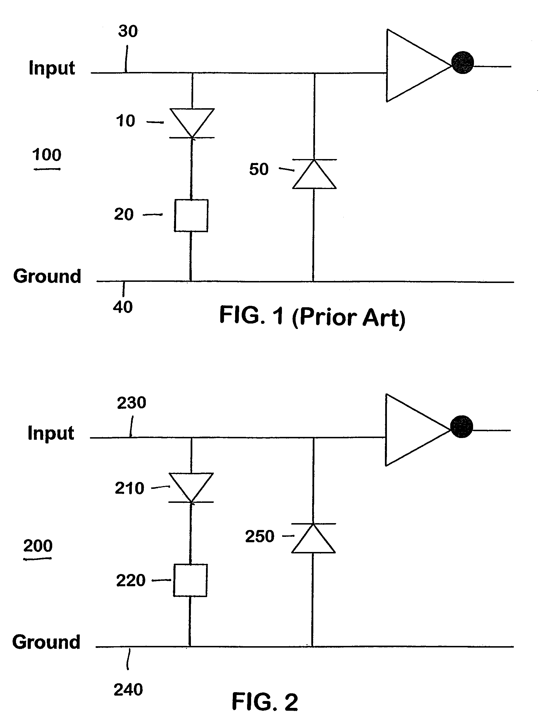
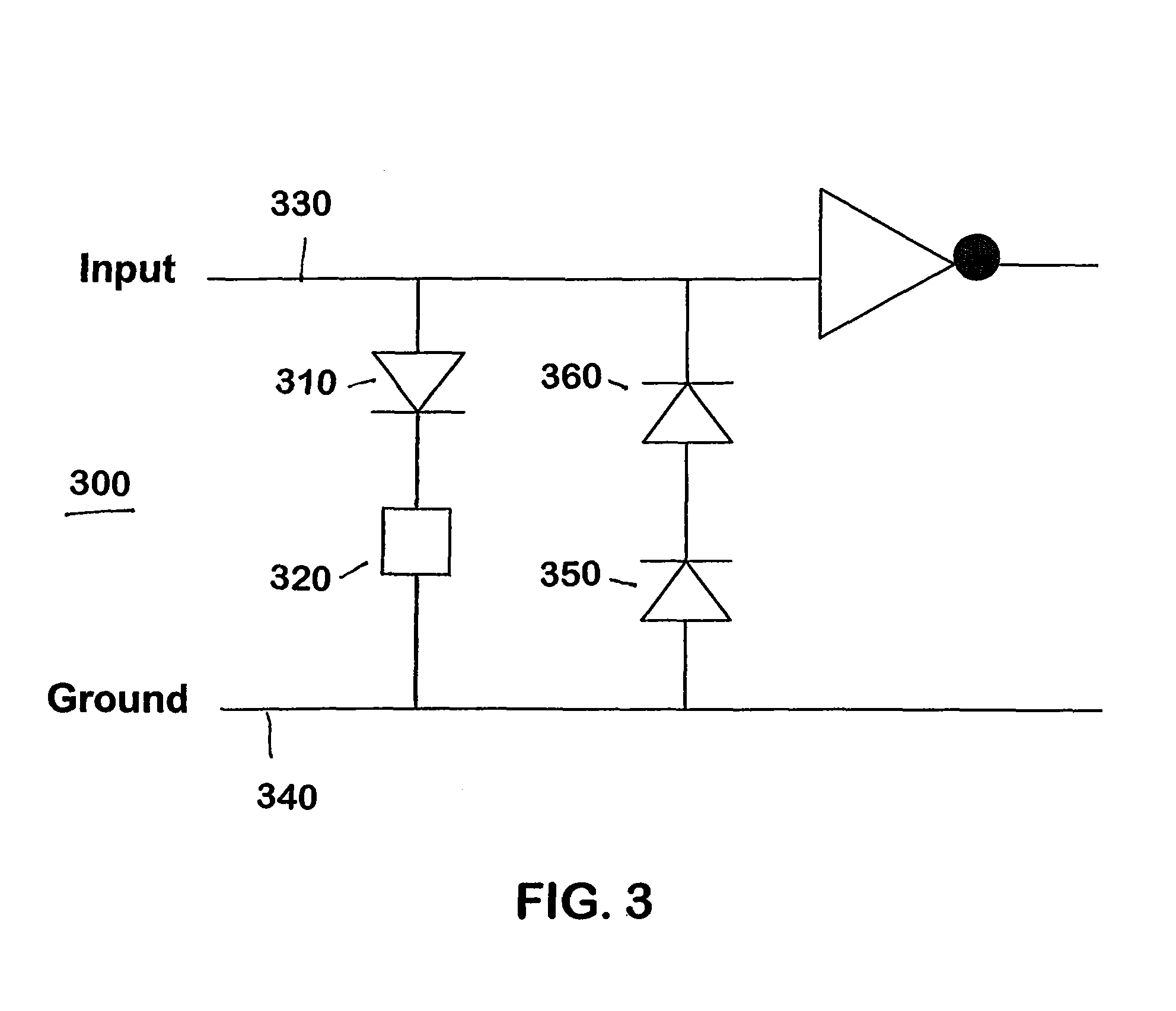
[0013]FIG. 2 is a schematic diagram of a first ESD protection circuit 200 of the present invention. Circuit 200 comprises a first diode 210 and a silicon controlled rectifier (SCR) 220 connected in series between an input node or lead 230 and a ground node 240 and a second diode 250 connected between input node 230 and ground node 240. An anode of the first diode 210 is connected to input node 230 and an anode of the second diode is connected to ground node 240. In this arrangement, a positive zap is discharged through the first diode and SCR; and a negative zap is discharged through the second diode.
[0014]In accordance with this embodiment of the invention, the capacitance of the second diode is reduced by forming the second diode from a PN junction between a heavily doped region of one conductivity type and a substrate region of the opposite conductivity type. The substrate is lightly doped or native and in any event is doped much less than the well region. Preferably, the heavily...
PUM
 Abstract
Description
Claims
Application Information
 - Generate Ideas
- Intellectual Property
- Life Sciences
- Materials
- Tech Scout
- Unparalleled Data Quality
- Higher Quality Content
- 60% Fewer Hallucinations
Browse by: Latest US Patents, China's latest patents, Technical Efficacy Thesaurus, Application Domain, Technology Topic, Popular Technical Reports.
© 2025 PatSnap. All rights reserved.Legal|Privacy policy|Modern Slavery Act Transparency Statement|Sitemap|About US| Contact US: help@patsnap.com