Double quench circuit for an avalanche current device

a technology of avalanche current and quench circuit, which is applied in the direction of amplifiers controlled by light, automatic control of pulses, amplifiers, etc., can solve the problems of large rc time constant, parasitic or intrinsic capacitance, and limited minimum interval between detectable events, so as to reduce the heating of the avalanche current device, reduce the after pulsing of the avalanche device, and fast reset the avalanche device

Active Publication Date: 2011-03-01
EXCELITAS CANADA
View PDF6 Cites 21 Cited by
  • Summary
  • Abstract
  • Description
  • Claims
  • Application Information

AI Technical Summary

Benefits of technology

[0008]It is a further object of this invention to provide such a double quench circuit which provides a faster reset of the avalanche device.
[0018]The invention also features a double quench circuit for an avalanche photodiode (APD), the circuit comprising, an avalanche photodiode having a cathode responsive to a bias voltage to reverse bias the APD above its avalanche breakdown voltage, a detection circuit including a comparator responsive to avalanche current of the APD and a reference voltage for detecting the avalanche current and generating an output signal in response thereto, a passive quench circuit including one or more resistors responsive to the bias voltage and coupled to the cathode of the APD for reducing the amount of the avalanche current passing through the APD, an active quench circuit responsive to the detection circuit and coupled to the anode of the APD for reducing the avalanche breakdown voltage to quench the avalanche current of the avalanche, a first active reset circuit responsive to the output signal of the detection circuit, said active reset circuit configured to couple the cathode to the voltage source to recharge the APD above its avalanche breakdown voltage to reset the APD and a second active reset circuit responsive to the output signal of the detection circuit and connected to the anode of the avalanche device, said second active reset circuit configured to couple the anode to a third voltage to recharge the avalanche device above its avalanche breakdown voltage to reset the avalanche device.

Problems solved by technology

While using this circuitry, the minimum interval between detectable events is limited by the so-called “dead time”: the time required to turn off the diode completely and to recharge it, and any other parasitic or intrinsic capacitance associated with the diode, through the typically large current limiting resistor which results in a large RC time constant.
Although this reduces the “dead time” by circumventing the RC time constant delay suffered by the passive quench circuits, it may introduce parasitic or intrinsic capacitance.
Additionally, the use of a traditional active quench circuit can also be disadvantageous since it creates a time delay in the circuit.
Thus, the using an active quench circuit on both the anode and cathode sides of an APD is not typically desirable.

Method used


Image

  • Double quench circuit for an avalanche current device
  • Double quench circuit for an avalanche current device
  • Double quench circuit for an avalanche current device

Examples


Embodiment Construction

[0029]Aside from the preferred embodiment or embodiments disclosed below, this invention is capable of other embodiments and of being practiced or being carried out in various ways. Thus, it is to be understood that the invention is not limited in its application to the details of construction and the arrangements of components set forth in the following description or illustrated in the drawings. If only one embodiment is described herein, the claims hereof are not to be limited to that embodiment. Moreover, the claims hereof are not to be read restrictively unless there is clear and convincing evidence manifesting a certain exclusion, restriction, or disclaimer.

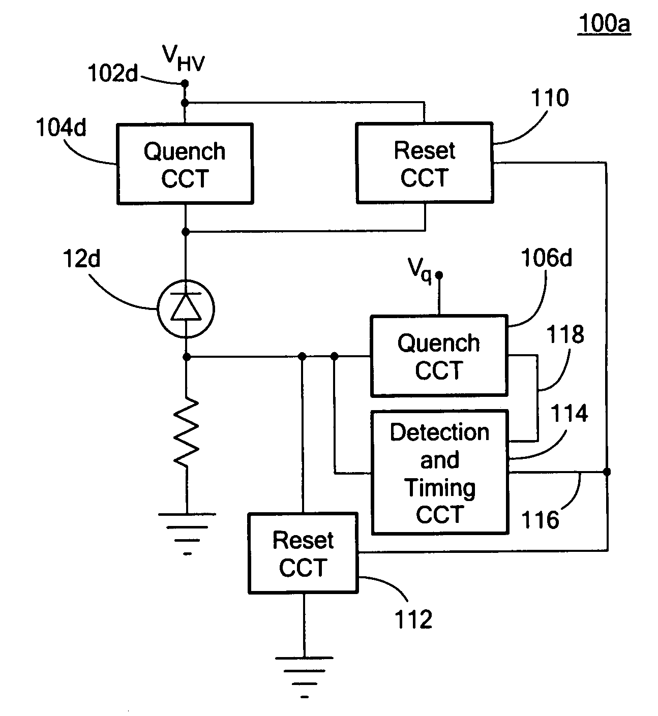
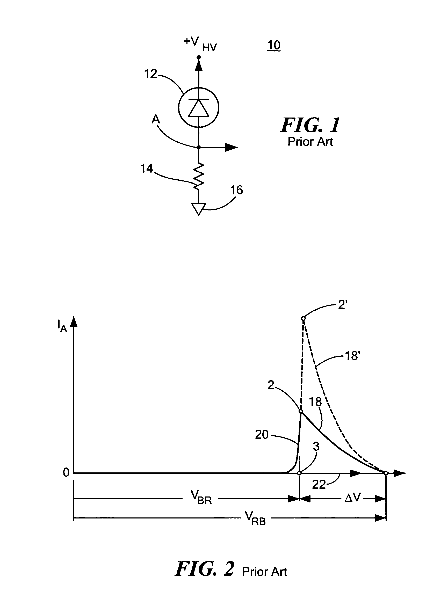
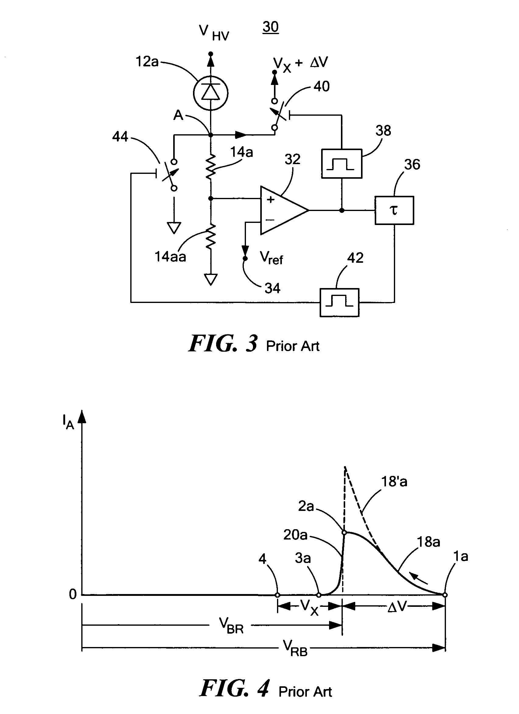
[0030]There is shown in FIG. 1 one prior art passive quench circuit 10 including an avalanche diode 12 and a biasing resistor 14. Resistor 14 is connected at junction A to the anode of avalanche device 12 and at its other end connected to ground 16. The cathode of avalanche current device 12 is connected to a high voltage V...


PUM


Abstract

A double quench circuit for an avalanche current device is provided in which the circuit includes an avalanche current device having a first terminal responsive to a bias voltage to reverse bias the avalanche current device above its avalanche breakdown voltage. A first quench circuit is responsive to the bias voltage and coupled to the first terminal of the avalanche device for reducing the amount of the avalanche current passing through the avalanche device. A second quench circuit is coupled to a second terminal of the avalanche device for reducing the amount of the avalanche current passing through the avalanche device.

Description

FIELD OF THE INVENTION[0001]This invention relates to a double quench circuit for an avalanche current device, and more particularly to passive and active quench circuits for avalanche photodiodes.BACKGROUND OF THE INVENTION[0002]Photodiodes convert light into electricity and thus can be used to detect light levels. An avalanche photodiode (APD) is a semiconductor device that can detect extremely low levels of electromagnetic radiation. Unlike a PIN photodiode, which generally produces a single electron for each photon received, an APD is constructed so that an electron dislodged by a photon will hit other atoms in the APD semiconductor lattice with sufficient velocity and energy so that additional hole-electron pairs are created by the collisions. Typically a free electron will create a number of hole-electron pairs, and the electrons from these pairs will, in turn, create additional electrons, thus creating an “avalanche” process. This multiplication of the electrons gives the APD...

Claims


Application Information

Patent Timeline
Patent Type & Authority Patents(United States)
IPC IPC(8): H01J40/14
CPCH03K17/0416H03K17/28H03K17/6877H03K17/78H01L31/107H03K17/06H03K17/60H03K2017/066H03K2017/0806
Inventor DESCHAMPS, PIERRE D.
Owner EXCELITAS CANADA
Why Eureka
Try Eureka