Integrated on-chip inductors and capacitors for improved performance of an optical modulator

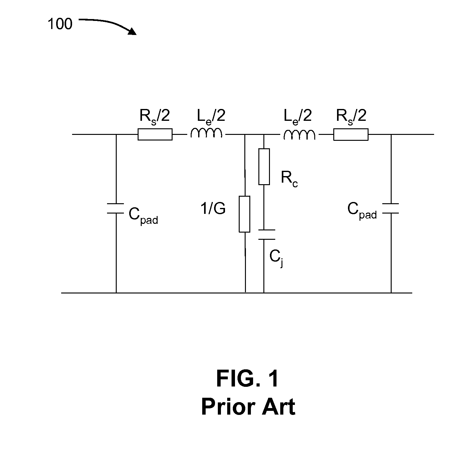
a technology of capacitors and inductors, applied in the field of modulators, can solve the problems of reducing the bandwidth of optical output signals, affecting the performance of optical modulators, and affecting the performance of optical modulators, and reducing the amount of series inductance, which can be provided by such microstrip lines,

Active Publication Date: 2011-03-01
LUMENTUM OPERATIONS LLC
View PDF6 Cites 7 Cited by
  • Summary
  • Abstract
  • Description
  • Claims
  • Application Information

AI Technical Summary

Problems solved by technology

When the outputs of the two waveguides are coherently combined in an optical coupling region, the resulting interference produces a change in amplitude of the combined optical signal.
An increase in velocity mismatch tends to reduce the bandwidth of the optical output signal.
However, the amount of series inductance, which such microstrip lines can provide, is limited by the space on top of the ridge 50 as well as the impedance per length of the microstrip lines 55.
Generally this requires more bond wires, whose electrical characteristics, in particular inductance values, are difficult to control, as well as additional bond pads, each of which contribute additional shunt capacitance.
Furthermore, with velocity-matched and similar designs, however, additional filters are often required for increasing the roll-off characteristics of the signal channel bandwidth to avoid interference and cross-talk with neighboring channels.
Such additional filters can increase losses, reduce efficiency and contribute to increased size and complexity of the device.

Method used


Image

  • Integrated on-chip inductors and capacitors for improved performance of an optical modulator
  • Integrated on-chip inductors and capacitors for improved performance of an optical modulator
  • Integrated on-chip inductors and capacitors for improved performance of an optical modulator

Examples


first embodiment

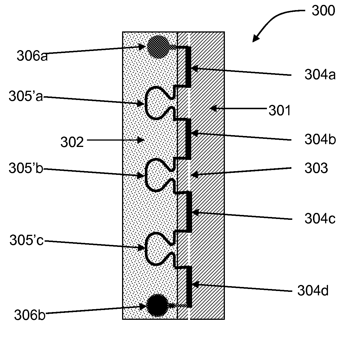
[0059]A first embodiment comprising on-chip inductors to improve modulator performance is shown in plan view in FIG. 3(a). A conducting layer 301, typically n-doped, on modulator chip 300 extends to one side from under a ridge waveguide 303 for providing a connection from an n-side of a p-n junction (310 in FIG. 3(c)) within the ridge waveguide 303 to a metal ground electrode (not shown). An insulating layer 302 extends over the rest of the modulator chip 300 up to the other side of the ridge waveguide 303. The insulating layer 302 may consist of layers of semi-insulating semiconductor materials, or layers of dielectric material, or a combinations of both. The conducting layer 301 may also extend partly or completely underneath insulating layer 302.

[0060]Conducting electrode segments 304a-d are disposed on top of the ridge waveguide 303 for providing a signal electrode connection to the p-n junction (310 in FIG. 3(c)) within the ridge waveguide 303. The length and number of the sign...

second embodiment

[0065]FIG. 3(c) is a cross-section of the second embodiment along section A-A′ in FIG. 3(b). As in FIG. 3(b), the modulator chip 300 comprises the substrate 330 with the conducting layer 301, preferably of semiconductor material, extending over a part or whole of the surface area of the substrate 330. A modulator diode 310 comprising a p-n junction within an optical ridge waveguide 303 is electrically connected to the conducting layer 301 and a traveling wave electrode 311 on top of the optical ridge waveguide 303. The modulator diode 310 layer structure may contain an intrinsic layer, single or multiple quantum wells as well as a p-type and n-type semiconductor region designed according to the required electro-optic characteristics for the modulator function.

[0066]The traveling wave electrode 311 is connected by means of the taps 312a-d or other suitable bridge contact structure to the inductors 305a-e situated on the insulating layer 302.

[0067]The substrate 330 is preferably insul...


PUM

PropertyMeasurementUnit
total lengthaaaaaaaaaa
inductanceaaaaaaaaaa

Abstract

An optical modulator for fiberoptic telecommunications is disclosed in which the optical signal velocity in the modulator waveguide and the electrical signal velocity in the traveling wave signal electrode are purposely mismatched by a factor of up to about 4. On-chip integrated inductors and capacitors are implemented to achieve the velocity mismatch. Improved electro-optic characteristics, such as return loss and sharper cut-off bandwidth are obtained.

Description

CROSS-REFERENCE TO RELATED APPLICATIONS[0001]The present invention claims priority from U.S. Provisional Patent Application No. 61 / 056,743 filed May 28, 2008, which is incorporated herein by reference.TECHNICAL FIELD[0002]The present invention is directed to modulators, and more particularly, to integrated electro-optical modulators with velocity mismatched traveling wave electrodes.BACKGROUND OF THE INVENTION[0003]Optical-fiber communication systems may include a transmitter with, for example, a high power, low noise laser source whose optical output is modulated with a wide bandwidth external modulator. Integrated electro-optical modulators are finding increasing use to reduce component physical size while increasing performance. To fabricate an integrated electro-optical modulator, a common substrate material for both the laser and modulator is generally required. Laser sources have been typically fabricated on compound semiconductor materials, to which the optical modulator need...

Claims


Application Information

Patent Timeline
Patent Type & Authority Patents(United States)
IPC IPC(8): G02F1/35
CPCG02F1/0121G02F1/0356G02F1/2255G02F2001/212G02F1/212
Inventor KOH, PING-CHIEK
Owner LUMENTUM OPERATIONS LLC
Why Eureka
Try Eureka