Printable electric circuits, electronic components and method of forming the same

a technology of electronic components and printed circuits, applied in the field of electronic circuits, to achieve the effect of reducing costs and being easy to controllabl

Inactive Publication Date: 2011-03-08
SILURIA TECH INC
View PDF60 Cites 53 Cited by
  • Summary
  • Abstract
  • Description
  • Claims
  • Application Information

AI Technical Summary

Benefits of technology

[0099]A variety of materials can be used for the substrate, presenting a surface for disposition of the seed layer, including electrically conductive, semiconductive, or insulative materials. The substrates may include metals, such as thin stainless steel sheets. They may also include prefabricated epoxy resin circuit boards. The substrate may be a semiconductor of any selected desired choice, such as silicon, gallium arsenide, germanium, or other material. Other acceptable substrates include plastics, polyimide layers, a flexible polymer sheet, an insulator, ceramic, laminate substrates, or multilayer substrates composed of any of the other variety of other materials. One advantage of the present invention is the ability to form an electrical circuit on a wide variety of acceptable substrates. One shortcoming of the prior art is the difficulty of forming electrical circuits on certain types of substrates. While epoxy resins are well developed for use as substrates, there is considerably more difficulty in the art using certain types of plastics, glasses, ceramics, or insulators as substrates. The substrate may be a flexible organic layer. For example, it may be a fiber, fabric, cloth, or plant, including a living plant, such as the leaf of a tree. Current technology does not permit the formation of electrical circuits on living plants based on the need to expose to harsh chemicals and high temperature steps. The present invention permits the formation of electrical circuits at room temperature, thus permitting the formation the electrical circuit on a much wider range of substrates than is possible in the prior art. Any substrate on which a pattern may be printed is usable as a substrate in the present invention, thus including practically all possible materials.
[0100]The substrates can include multilayer substrates. The substrate can be, for example, glass, quartz, oxide or nitride material, plastic, ceramic, semiconductor such as silicon, germanium, and the like, conductor such as aluminum, composites of materials including metals and semiconductors, and multilayer coating of any of these materials.
[0101]The substrates are typically those where a metal film would be grown, including for example Ta, TaN, Ti, TiN, TiW, Mo, Cr, silicon oxide (including silicon dioxide), silicon nitride, silicon oxynitride. These substrates can be, for example, barrier materials which prevent copper diffusion. The substrates may be cleaned, prepared, or coated with a oxide or other substance. In a preferred embodiment, the system is used where the peptide is directly bound without any coating on the substrate in order to direct the metal film directly on the desired layer.
[0102]Substrates also can be selected for usefulness in displays including liquid crystal displays. Deposition of seed layers on glass substrates is described in U.S. Pat. No. 6,887,776, which is hereby incorporated by reference in their entirety. Glasses include undoped silica glass (USG), phosphorous doped glass (PSG), boron-phosphorous doped glass (BPSG), soda-lime glass, borosilicate glass, sodium borosilicate glass, alkali-metal borosilicate, aluminosilicate glass, aluminoborosilicate glass, alkaline earth aluminoborosilicate glass, alkaline earth-metal aluminoborosilicate glass, and combinations thereof.Printing
[0103]The present invention permits the printing to be carried out by any currently known printing technique. The printing technique which may be used includes inkjet printing. Inkjet printing is well developed in the art, and numerous solutions having different viscosities have been adapted to inkjet printing. lnkjet printing is also very versatile in providing a wide range of patterns to be printed having various widths and dimensions easily controllable by software. Use of inkjet printing provides a substantial advantage over current techniques for printing circuit boards. With the use of an inkjet printer, the printer can be driven by appropriate software electronics to form the desired pattern. Thus, a mask layer followed lithography processing is not necessary with the present invention. The substrate 12 on which the pattern is to be formed can be simply printed using inkjet printing—in a desired pattern at substantially lower costs than is currently permitted using the expensive masks, exposed etch and treat techniques common in the art today. Other types of printing may also be used. For example, gravure printing, which has advantages for certain substrates and for forming selected patterns. Laser printing, thermal transfer, laser induced thermal transfer, flexo printing, and offset printing may also be used. The present invention is also useful for all methods of lithography.
[0104]Inkjet printing also permits different seed layers to be printed at the same time using standard inkjet printing techniques. This will assure self-alignment of the various seed layers. This is accomplished as follows. It is known to print three or four colors in a single printing with an inkjet printer, such as red, blue, yellow, and sometimes also black. This is carried out today with a single ink cartridge having the three or four inkwells therein.

Problems solved by technology

In addition, the expensive equipment and capital investment required in order to form an electronic circuit on the given substrate is not necessary.

Method used


Image

  • Printable electric circuits, electronic components and method of forming the same
  • Printable electric circuits, electronic components and method of forming the same
  • Printable electric circuits, electronic components and method of forming the same

Examples


Embodiment Construction

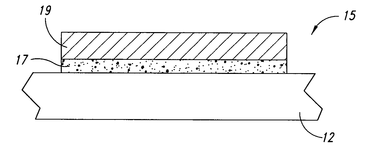
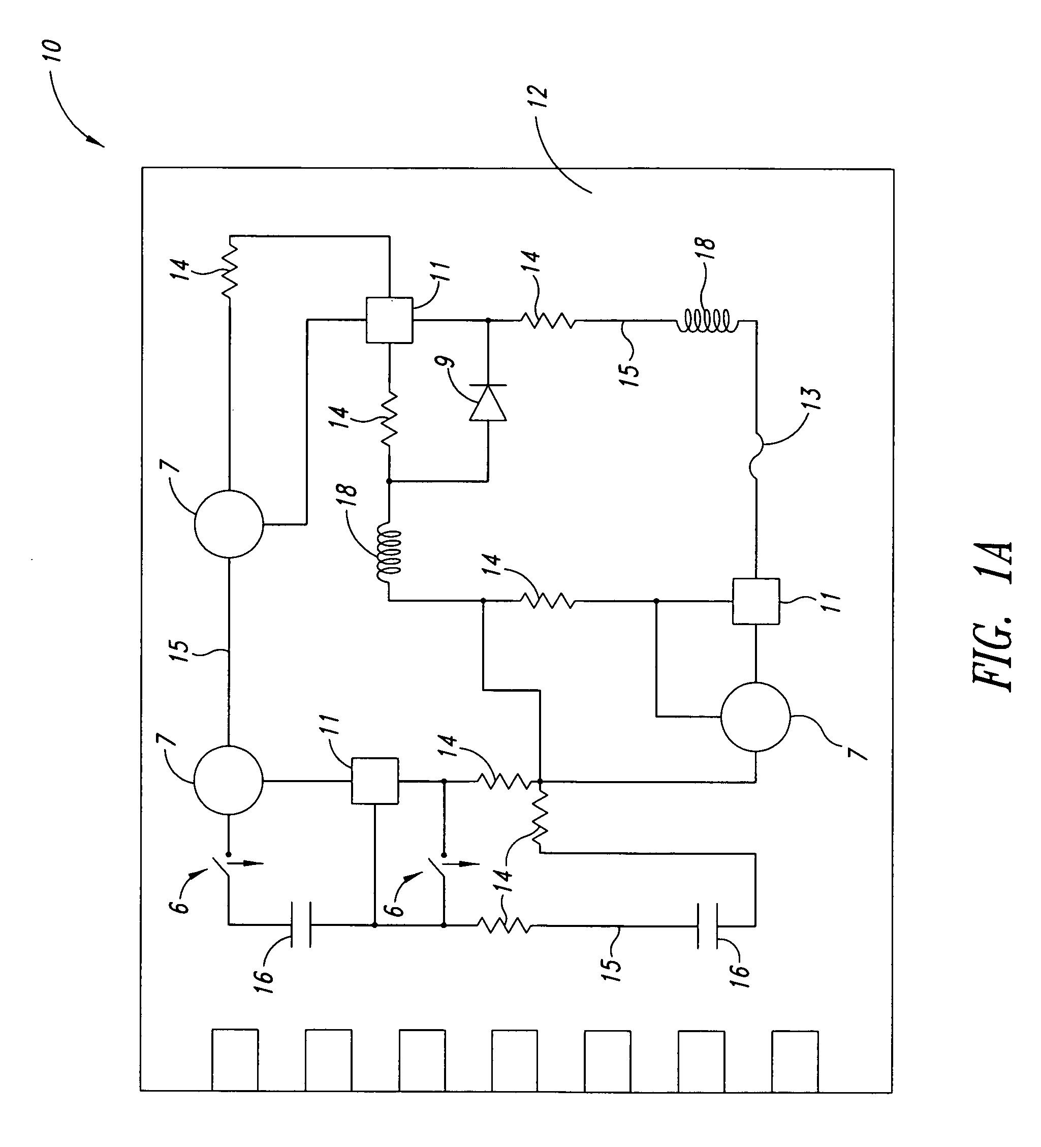
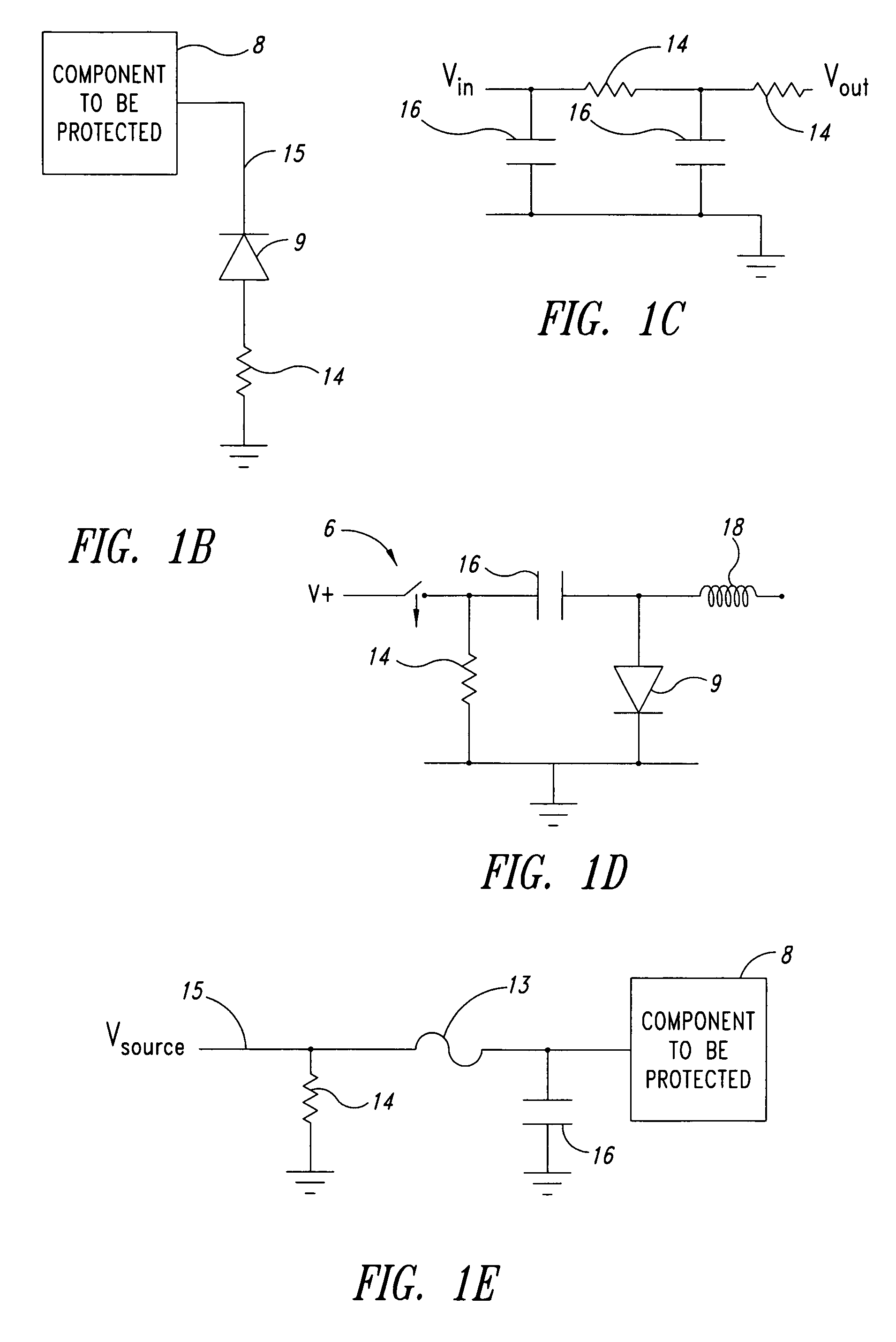
[0064]FIG. 1A illustrates examples of various components that can be formed in a circuit 10 which has been constructed according to principles of the present invention. The circuit 10 includes a substrate 12 having an electrical connection which includes a variety of electrical components. Passive components may include fuse 13, resistors 14, capacitors 16, and one or more inductors 18. In some embodiments, only passive components are provided on the printed circuit. In other embodiments, one or more active components may be included on the circuit. The active components which may be included are a diode 9, or various other active components 7 and 11 which may be selected according to the needs of a particular circuit.

[0065]The circuit presented in FIG. 1A is provided for illustration purposes to demonstrate the variety of electrical components which can be electrically coupled to each other according to principles of the present invention and is not intended to illustrate the actua...


PUM

PropertyMeasurementUnit
particle sizeaaaaaaaaaa
temperatureaaaaaaaaaa

Abstract

Improved methods and articles providing conformal coatings for a variety of devices including electronic, semiconductor, and liquid crystal display devices. Peptide formulations which bind to nanoparticles and substrates, including substrates with trenches and vias, to provide conformal coverage as a seed layer. The seed layer can be further enhanced with use of metallic films deposited on the seed layer. Seed layers can be characterized by AFM measurements and improved seed layers provide for better enhancement layers including lower resistivity in the enhancement layer. Peptides can be identified by phage display.

Description

STATEMENT OF GOVERNMENT INTEREST[0001]This invention was made with government support under Contract No. 2004-H838109-000 awarded by the Central Intelligence Agency. The government has certain rights in this invention.BACKGROUND OF THE INVENTION[0002]1. Field of the Invention[0003]This invention relates to electronic circuits that are formed by printing on a substrate, and more particularly, to a method of fabricating electronic circuits having active and passive components on any substrate by adhering to a seed layer that has been printed on the substrate.[0004]2. Description of the Related Art[0005]Substrates having electrically conductive lines thereon are used in a wide variety of electronic applications. Glass substrates used for LCD's, touch screens for visual displays, consumer electronic displays, from cell phone to portable computers all require electrically conductive lines to be formed thereon to provide the desired functionality. Flexible substrates are also used in a wi...

Claims


Application Information

Patent Timeline
Patent Type & Authority Patents(United States)
IPC IPC(8): H01L29/40
CPCH05K1/162H05K1/165H05K1/167H05K3/389C23C18/1879C23C18/1889C23C18/1608C23C18/1639C23C18/208C23C18/30C23C18/1692C23C18/206B82Y10/00B82Y30/00G02F1/136204H05K3/105H05K3/12H05K2201/0209H05K2201/0257H05K2201/086H05K2203/0545H05K2203/122
Inventor GARROU, PHILIP E.KNAPP, MICHAEL R.PAKBAZ, HASHPSCHENITZKA, FLORIANQUAN, XINASPAID, MICHAEL A.
Owner SILURIA TECH INC
Why Eureka
Try Eureka