Method of manufacturing the organic electroluminescent display and organic electroluminescent display manufactured by the method

a technology of organic electroluminescent display and manufacturing method, which is applied in the direction of vacuum evaporation coating, solid-state devices, coatings, etc., can solve the problems of increasing the manufacturing increasing the production cost of the substrate, and reducing the yield of the manufacturing method, so as to suppress the generation of foreign substances, the effect of reducing the production cost and suppressing the deterioration of the properties of the thin film

Active Publication Date: 2011-03-29
SAMSUNG DISPLAY CO LTD +1
View PDF12 Cites 4 Cited by
  • Summary
  • Abstract
  • Description
  • Claims
  • Application Information

AI Technical Summary

Benefits of technology

[0017]In the conventional method which vapor-deposits the organic film such as the light emitting layer of the organic EL to the predetermined portion of the substrate by adhering the vapor deposition mask to the substrate, there have been drawbacks such as (1) the vapor deposition mask is adhered to the substrate and hence, the formed organic film such as the OLED film is easily damaged, (2) the vapor deposition mask is continuously formed on the substrate and the vapor deposition mask and hence, when film peeling-off is generated at the time of peeling off the vapor deposition mask and the substrate from each other and this peeling-off generates foreign substances, (3) the substrate and the vapor deposition mask are easily influenced by difference in thermal expansion coefficient between the substrate and the vapor deposition mask and hence, the substrate and the vapor deposition mask rub each other thus generating damages and foreign substances, and (4) it is difficult to completely adhere the vapor deposition mask to the whole substrate and hence, it is often the case that the distribution of vapor-deposition accuracy in the inside of the substrate is increased or a fine pattern portion is twisted.
[0018]Among the countermeasures which are disclosed in the above-mentioned Patent Documents, the method which forms the ribs or the projections on the substrate pushes up a manufacturing cost of the substrate. On the other hand, a mechanical damage reduction effect is small. In the method which forms irregularities on a surface of the vapor deposition mask, the preparation of the vapor deposition mask is difficult and hence, it is difficult to ensure the accuracy of vapor-deposition pattern. In both methods, the substrate and the vapor deposition mask are adhered to each other in an effective area of the display panel and hence, it is difficult to suppress the generation of damages and foreign substances of the organic film such as the OLED film on the portion. Here, although there has been also known a method which performs the vapor deposition while separating the vapor deposition mask and the substrate from each other, it is extremely difficult to align the vapor deposition mask and the substrate in this method.
[0019]Accordingly, it is an object of the present invention to provide a method of manufacturing an organic EL display panel which can form a desired organic film or the like with high accuracy without damaging the substrate or the organic film and an organic EL display panel which is manufactured by the method.

Problems solved by technology

In the conventional method which vapor-deposits the organic film such as the light emitting layer of the organic EL to the predetermined portion of the substrate by adhering the vapor deposition mask to the substrate, there have been drawbacks such as (1) the vapor deposition mask is adhered to the substrate and hence, the formed organic film such as the OLED film is easily damaged, (2) the vapor deposition mask is continuously formed on the substrate and the vapor deposition mask and hence, when film peeling-off is generated at the time of peeling off the vapor deposition mask and the substrate from each other and this peeling-off generates foreign substances, (3) the substrate and the vapor deposition mask are easily influenced by difference in thermal expansion coefficient between the substrate and the vapor deposition mask and hence, the substrate and the vapor deposition mask rub each other thus generating damages and foreign substances, and (4) it is difficult to completely adhere the vapor deposition mask to the whole substrate and hence, it is often the case that the distribution of vapor-deposition accuracy in the inside of the substrate is increased or a fine pattern portion is twisted.
Among the countermeasures which are disclosed in the above-mentioned Patent Documents, the method which forms the ribs or the projections on the substrate pushes up a manufacturing cost of the substrate.
In the method which forms irregularities on a surface of the vapor deposition mask, the preparation of the vapor deposition mask is difficult and hence, it is difficult to ensure the accuracy of vapor-deposition pattern.
In both methods, the substrate and the vapor deposition mask are adhered to each other in an effective area of the display panel and hence, it is difficult to suppress the generation of damages and foreign substances of the organic film such as the OLED film on the portion.
Here, although there has been also known a method which performs the vapor deposition while separating the vapor deposition mask and the substrate from each other, it is extremely difficult to align the vapor deposition mask and the substrate in this method.

Method used


Image

  • Method of manufacturing the organic electroluminescent display and organic electroluminescent display manufactured by the method
  • Method of manufacturing the organic electroluminescent display and organic electroluminescent display manufactured by the method
  • Method of manufacturing the organic electroluminescent display and organic electroluminescent display manufactured by the method

Examples


embodiment 1

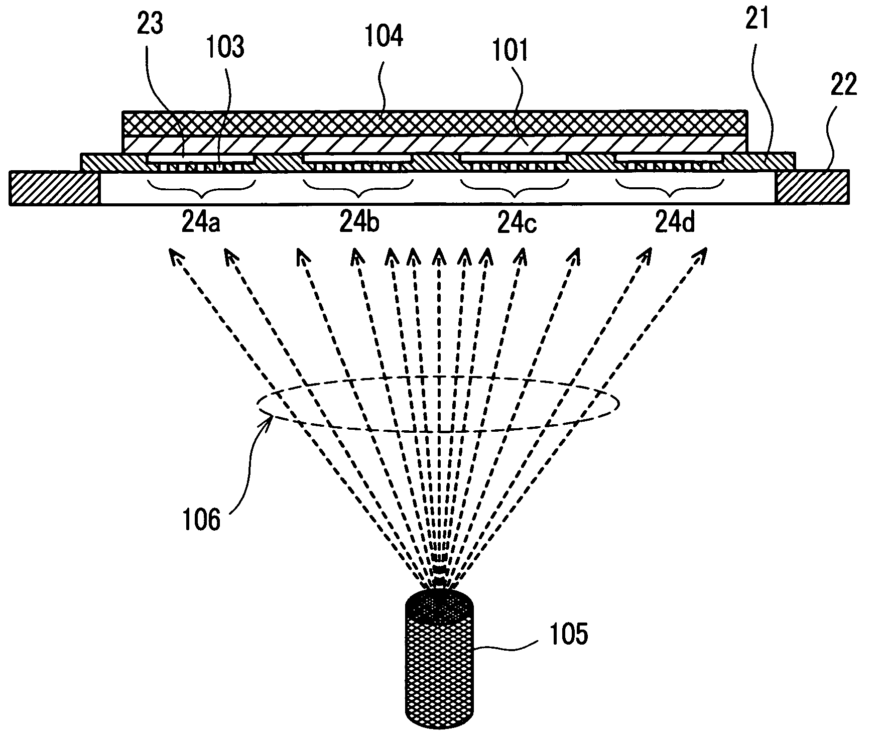
[0048]FIG. 1 a schematic view for explaining an embodiment 1 of a method of manufacturing an organic EL display panel according to the present invention. A substrate 101 is a TFT substrate which constitutes the organic EL display panel and is a base substrate which is formed of a glass plate. Here, it is assumed that n×m pieces of small-sized panels, that is, individual organic EL display panels (also simply referred to as a display panel) in which n pieces (four in FIG. 1) of display panels are arranged in the lateral direction on this paper and m pieces of display panels are arranged in the direction perpendicular to this paper are manufactured from the substrate 101. In FIG. 1, an effective area of the display panel is indicated as panel pattern portions 24 (24a, 24b, 24c, 24d).

[0049]The vapor deposition is performed in a state that a vapor deposition mask 21 having opening portions 103 is arranged on a main surface side of the substrate 101. In the embodiment 1, the vapor deposi...

embodiment 2

[0097]FIG. 8 is a schematic view for explaining an embodiment 2 of the method of manufacturing an organic EL display panel according to the present invention. FIG. 8 schematically shows a structural example of a vapor deposition mask and a vapor deposition pattern forming method using the vapor deposition mask in the embodiment 2. Here, a thin film layer which is formed on a vapor deposition mask and a substrate is omitted from the drawing. This embodiment differs from the embodiment 1 with respect to a point that the vapor deposition mask 51 has no mask frame for fixing. This embodiment is substantially equal to the embodiment 1 with respect to other constitutions.

[0098]The vapor deposition mask 51 and the substrate 101 are adhered to each other by an attraction force of the magnet 104. Also in this embodiment, a vapor deposition pattern is formed by way of a gap space 23 and hence, this embodiment can obtain advantageous effects substantially equal to the advantageous effects of t...

embodiment 3

[0100]FIG. 9 is a schematic view for explaining an embodiment 3 of the method of manufacturing an organic EL display panel according to the present invention. FIG. 9 schematically shows a structural example of a vapor deposition mask and a vapor deposition pattern forming method using the vapor deposition mask in the embodiment 3. Here, a thin film layer which is formed on a vapor deposition mask and a substrate is omitted from the drawing.

[0101]This embodiment 3 also differs from the embodiment 1, in the same manner as the embodiment 2, with respect to a point that a vapor deposition mask 61 is not fixed to the mask frame. The vapor deposition mask 61 and the substrate 101 are adhered to each other due to an attraction force of a magnet 104. In this embodiment 3, by increasing a plate thickness of a portion 65 which is adhered to the substrate 101 of the vapor deposition mask 61, it is possible to improve a mechanical strength compared to the embodiment 2. Accordingly, this embodim...


PUM

PropertyMeasurementUnit
temperatureaaaaaaaaaa
plate thicknessaaaaaaaaaa

Abstract

The present invention provides an organic EL display panel manufacturing method which is capable of forming a desired organic film or the like with high accuracy without imparting damages to a substrate and an organic film and an organic EL display panel which is manufactured by the method. An opening portion which corresponds to a panel pattern region of a display panel is formed in a vapor deposition mask. The opening portion has a bottom surface in the inside of a recessed surface which is retracted from a surface on which the vapor deposition mask is brought into contact with the substrate. The opening portion of the vapor deposition mask is spaced apart from the substrate with a predetermined gap space and evaporated particles from an evaporating source are vapor-deposited to the substrate through the opening portion.

Description

CROSS-REFERENCE TO RELATED APPLICATION[0001]The disclosure of Japanese Patent Application No. JP2005-279225 filed on Sep. 27, 2005 including the claims, the specification, the drawings and the abstract is incorporated herein by reference in its entirety.BACKGROUND OF THE INVENTION[0002]1. Field of the Invention[0003]The present invention relates to an organic EL display panel, and more particularly, to an organic EL display panel which is suitable for a method for manufacturing an organic thin film or an electrode film such as a light emitting layer on a substrate by vapor deposition using a vapor deposition mask in a predetermined pattern. The present invention is also characterized by the structure of the vapor deposition mask for such vapor deposition.[0004]2. Description of the Related Art[0005]FIG. 15 is a schematic view of a method of manufacturing an organic EL display panel for explaining a method for forming an organic film such as a light emitting layer using a vapor depos...

Claims


Application Information

Patent Timeline
Patent Type & Authority Patents(United States)
IPC IPC(8): H01L51/40
CPCC23C14/042C23C14/12H01L51/0011H01L51/56C23F1/02H10K71/166H10K71/00
Inventor MATSUZAKI, EIJITAKANOSU, KEIJIMATSUURA, HIROYASU
Owner SAMSUNG DISPLAY CO LTD
Why Eureka
Try Eureka