Photoelectric conversion device and manufacturing method thereof

a technology of photoelectric conversion and manufacturing method, which is applied in the direction of semiconductor/solid-state device manufacturing, semiconductor devices, electrical devices, etc., can solve the problems of increasing the difficulty of significantly reducing the cost of cell production, large volume of carbon dioxide emissions, and future supply deficiency of fossil fuels, and achieves high photoelectric conversion efficiency

Inactive Publication Date: 2011-03-29
SHARP KK
View PDF41 Cites 2 Cited by
  • Summary
  • Abstract
  • Description
  • Claims
  • Application Information

AI Technical Summary

Benefits of technology

[0020]It has been found that, by containing nitrogen atoms in a p-type or an n-type semiconductor layer in the above-mentioned pin-type photoelectric conversion layer, high photoelectric conversion efficiency can be obtained as compared to the case of containing no nitrogen atom in the either layer.
[0023]According to the photoelectric conversion device of an example embodiment, an open-circuit voltage and a short-circuit current are increased by containing nitrogen atoms, especially at a concentration of 0.001 to 10 atomic %, in a p-type semiconductor layer or an n-type semiconductor layer of a window layer on a light incident side, without containing a high-concentration impurity element in the p-type or n-type semiconductor layer, and thereby it is possible to improve photoelectric conversion efficiency, and further to enhance efficiency of a thin-film silicon solar cell.
[0024]Further, according to the manufacturing method of a photoelectric conversion device, it is possible to manufacture a photoelectric conversion device with high photoelectric conversion efficiency while significantly reducing input energy, as compared to a method for manufacturing a bulk-crystal type solar cell, thereby significantly suppressing a volume of carbon dioxide emissions during manufacturing.

Problems solved by technology

Due to a problem with a decrease in quantity of remaining resources, there has been a concern about future supply deficiency in fossil fuels, such as oil, that are utilized as power energy sources.
There has also been an issue with carbon dioxide emission that causes global warming.
However, since a bulk-crystal type solar cell is formed using a silicon substrate having a thickness of several hundreds of micrometers, raw material cost forms a large proportion of a price for a solar cell, and it is thus becoming more difficult to significantly reduce the cost of producing the cell.
This has caused a problem with a large volume of carbon dioxide emissions at the time of producing those silicon substrates.
However, since the thin-film silicon solar cell has low photoelectric conversion efficiency per unit area as compared to the bulk-crystal type solar cell, the market for the thin-film silicon solar cell has in reality not expanded like the market for the bulk-crystal type solar cell.
However, this involves a simultaneous increase in uncombined silicon in the film.
However, the above effect is not exerted throughout the ultimately obtained polycrystalline silicon thin film.
Namely, the foregoing effects of reduction in light absorption loss and improvement of an open-circuit voltage, produced by widening of a gap band, cannot be expected.
However, widening of the band gap of the n-type semiconductor layer has not been able to bring about production of an equivalent effect of improving photoelectric conversion efficiency to the effect achieved by widening the band gap of the p-type semiconductor layer.

Method used


Image

  • Photoelectric conversion device and manufacturing method thereof
  • Photoelectric conversion device and manufacturing method thereof
  • Photoelectric conversion device and manufacturing method thereof

Examples


embodiment 1

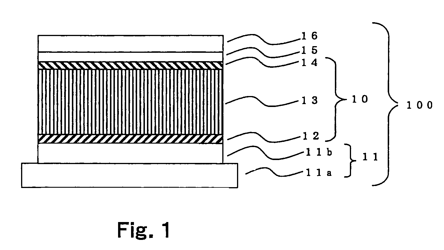
[0065]As shown in FIG. 1, a photoelectric conversion device 100 of Embodiment 1 has a superstrate type structure and is constituted by laminating, on a substrate 11, a photoelectric conversion layer 10, a transparent conductive layer 15, and an electrode 16, in this order.

[0066]The substrate 11 is produced by depositing, for example, a transparent conductive layer 11b on a light permeable substrate 11a. As the light permeable substrate 11a, a glass plate, a heat-resistant translucent plate of a resin such as polyimide or polyvinyl, or a lamination of those is preferably used. The light permeable substrate 11a is however not particularly restricted, as long as it has high translucency and can structurally support the entire photoelectric conversion device. The light permeable substrate 11a may also be produced by covering the above-mentioned plates with a light permeable metal film, a transparent conductive film, an insulating film, or the like. However, in the case of applying the p...

embodiment 2

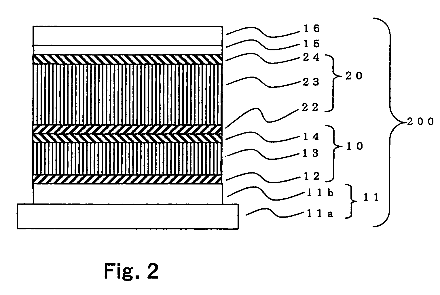
[0106]Next, a superstrate laminated type photoelectric conversion device 200 having two photoelectric conversion layers is described as Embodiment 2, a different embodiment from the above, using FIG. 2. It is to be noted that in FIG. 2, the same constituents as those of Embodiment 1 shown in FIG. 1 are provided with the same reference numerals as in FIG. 1.

[0107]This superstrate laminated type photoelectric conversion device 200 is constituted by laminating, on a substrate 11, a first photoelectric conversion layer 10, a second photoelectric conversion layer 20, a transparent conductive layer 15, and an electrode 16, in this order. Among these constituents, the substrate 11, the transparent conductive layer 15 and the electrode 16 can be the same ones as those used for the foregoing superstrate type photoelectric conversion device 100 can be used, and the functions of the respective layers are also the same as those of the superstrate type photoelectric conversion device 100. Hence ...

examples 10 to 14

[0124]In Examples 10 to 14, the superstrate type photoelectric conversion device 100 was manufactured in the following manner under the same conditions as in Examples 1 to 9 except for conditions for forming the p-type semiconductor layer 12.

[0125]The p-type semiconductor layer 12 was formed by forming a first p-type semiconductor layer, containing nitrogen atoms in the same concentration range as that in each of Examples 5 to 8, on the substrate 11 and then depositing a second p-type semiconductor layer, containing no nitrogen, on the first p-type semiconductor layer. In formation of the first p-type semiconductor layer, a gas flow rate ratio ([H2] / [SiH4]) was 150, and other layer formation conditions were shown in Table 1. In formation of the second p-type semiconductor layer, SiH4, H2 and B2H6 were used as raw material gases. A gas flow rate ratio ([H2] / [SiH4]) was 150, and a gas flow rate ratio ([B2H6] / [SiH4]) was shown in Table 1. The thicknesses of the first and second p-type ...


PUM


Abstract

A photoelectric conversion device comprising: a pin-type photoelectric conversion layer constituted of a p-type semiconductor layer, an i-type semiconductor layer and an n-type semiconductor layer, wherein the p-type semiconductor layer contains silicon atoms and nitrogen atoms, which is possible to improve photoelectric conversion efficiency.

Description

CROSS-REFERENCE TO RELATED APPLICATION[0001]This application is related to Japanese patent applications Nos. 2004-086811, 2004-257181 and 2004-308381, filed on 24 Mar. 2004, 3 Sep. 2004 and 22 Oct. 2004, respectively, whose priorities are claimed under 35 USC §119, the disclosures of which are incorporated by reference in their entirety.BACKGROUND[0002]1. Field of the Technology[0003]The technology presented herein relates to a photoelectric conversion device and a manufacturing method thereof. More specifically, the technology relates to a photoelectric conversion device with improved photoelectric conversion efficiency and a manufacturing method thereof.[0004]2. Description of the Related Art[0005]Due to a problem with a decrease in quantity of remaining resources, there has been a concern about future supply deficiency in fossil fuels, such as oil, that are utilized as power energy sources. There has also been an issue with carbon dioxide emission that causes global warming. Unde...

Claims


Application Information

Patent Timeline
Patent Type & Authority Patents(United States)
IPC IPC(8): H01L31/00H01L31/042H01L31/075H01L31/18
CPCH01L31/075Y02E10/548Y02E10/52H01L31/18
Inventor NISHIMURA, KAZUHITONASUNO, YOSHIYUKIYAMAMOTO, HIROSHISUGITA, YOSHITAKA
Owner SHARP KK
Why Eureka
Try Eureka