

Linearity improvements of semiconductor substrate using passivation
a technology of semiconductor substrates and passivation, applied in the direction of semiconductor devices, diodes, electrical apparatus, etc., can solve the problems of non-linear capacitance, non-linear conductance, non-linear capacitance, affecting the rf interaction between the silicon substrate and other layers, and achieving the effect of effectively immobilizing the surface conduction layer, preventing capacitance and inductance changes, and high density of traps
- Summary
- Abstract
- Description
- Claims
- Application Information
AI Technical Summary
Benefits of technology
Problems solved by technology
Method used
Image

Examples
Embodiment Construction
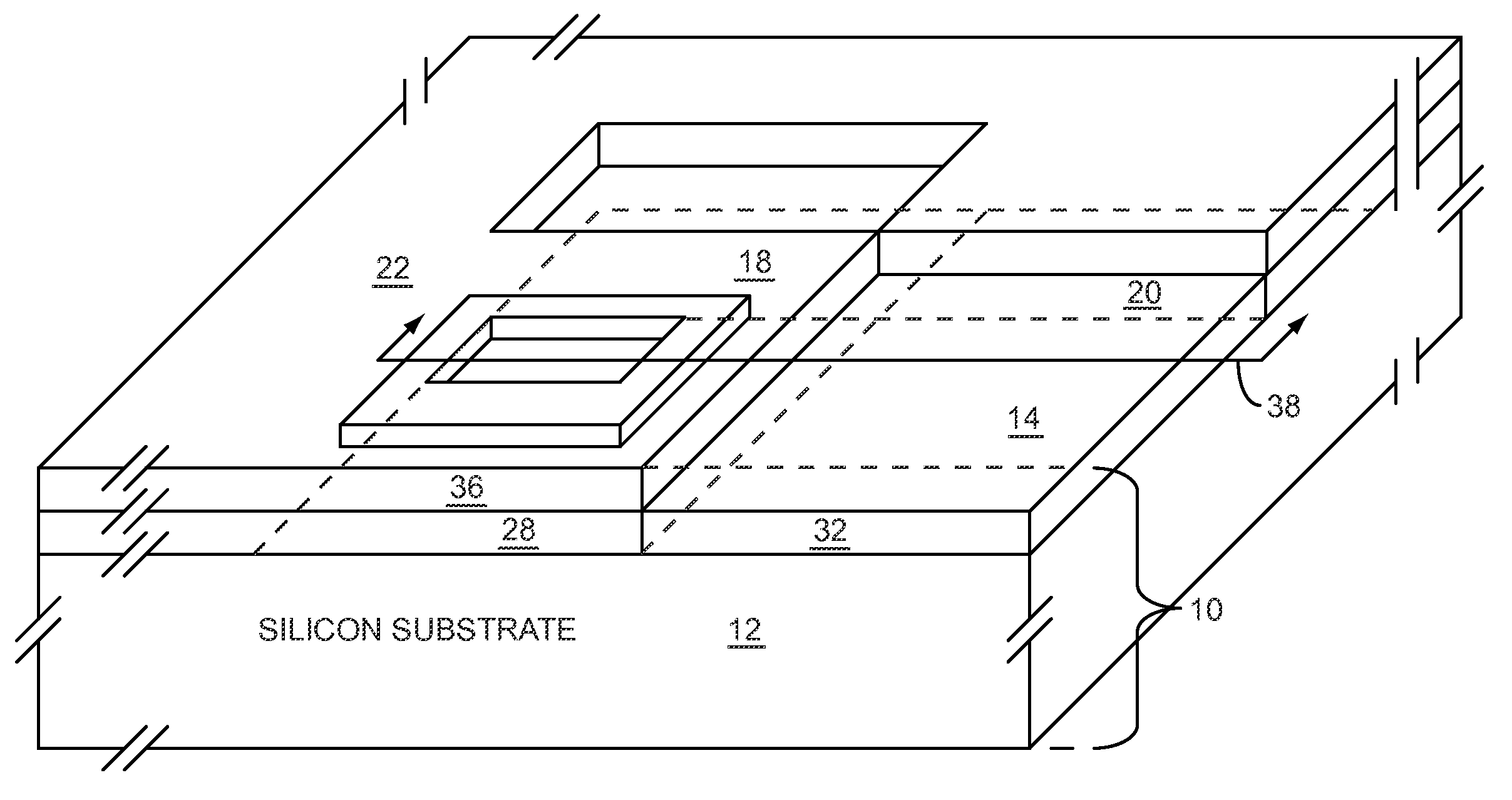
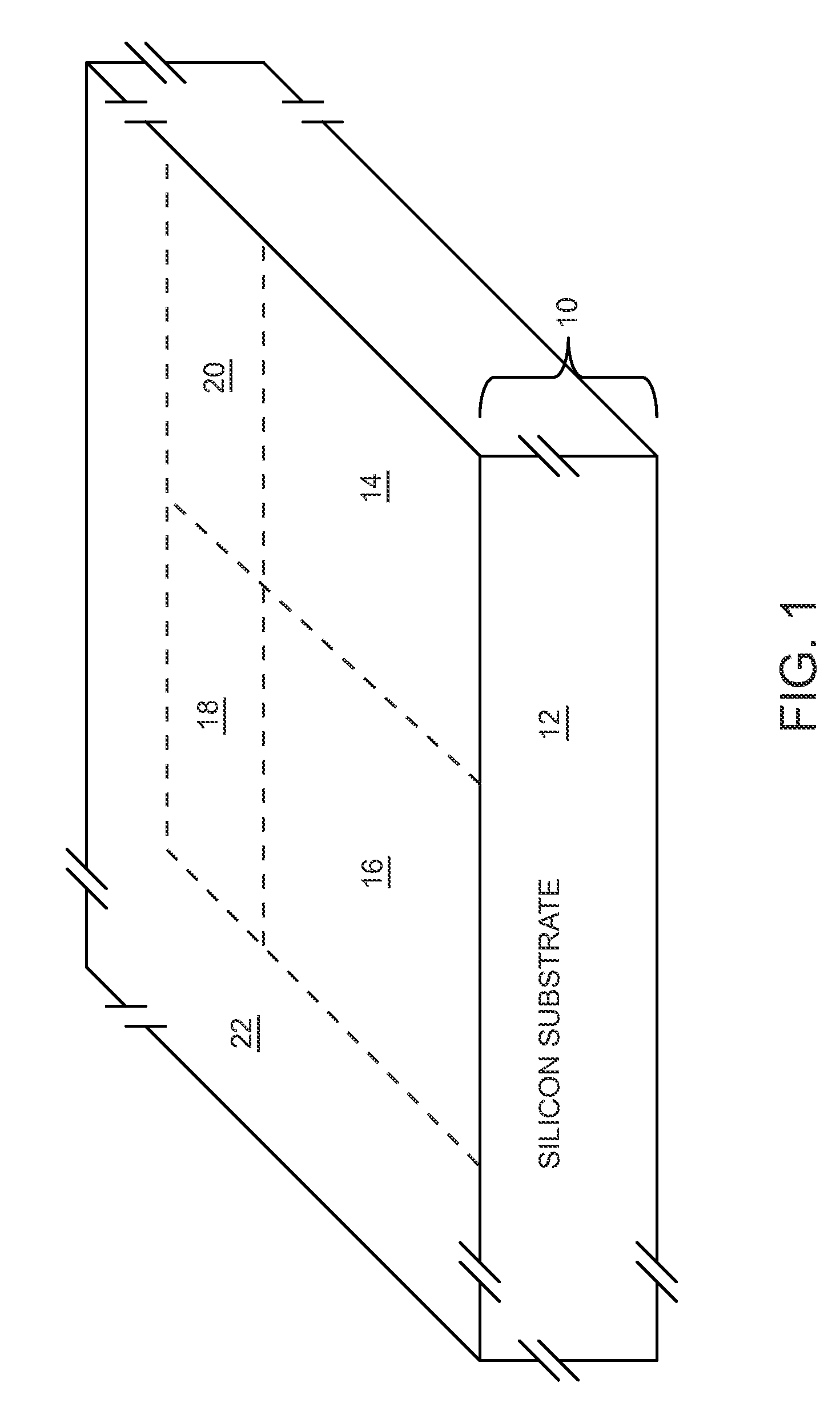
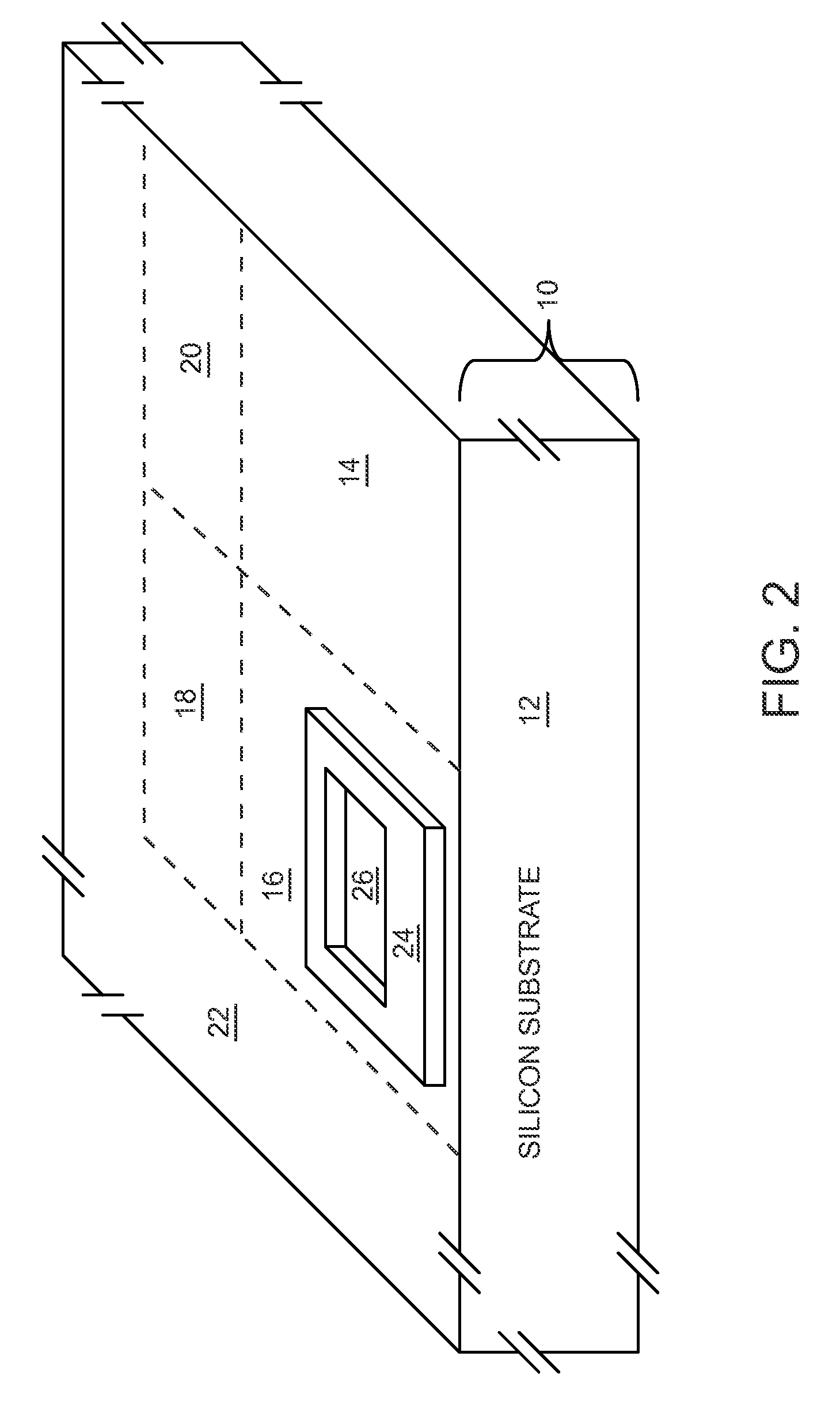
[0006]The present invention relates to using a potentially trap-rich layer, such as a polycrystalline Silicon layer, over a passivation region of a semiconductor substrate or a Silicon-on-insulator (SOI) device layer to substantially immobilize a surface conduction layer at the surface of the semiconductor substrate or SOI device layer at radio frequency (RF) frequencies. The potentially trap-rich layer may have a high density of traps that trap carriers from the surface conduction layer. The average release time from the traps may be longer than the period of any present RF signals, thereby effectively immobilizing the surface conduction layer, which may substantially prevent capacitance and inductance changes due to the RF signals. Therefore, harmonic distortion of the RF signals may be significantly reduced or eliminated. The semiconductor substrate may be a Silicon substrate, a Gallium Arsenide substrate, or another substrate.
[0007]The semiconductor substrate or SOI device layer...
PUM
 Abstract
Description
Claims
Application Information