

Microelectronic assembly with impedance controlled wirebond and conductive reference element
a technology of impedance control and microelectronic assembly, which is applied in the direction of electrical apparatus, semiconductor devices, and semiconductor/solid-state device details, etc., can solve the problems of electrical impedance problems, unwanted radiation and detuning of lines, and wire-bonds generally are also subject to self-inductance, and can be subject to external noise, etc., to achieve easy consumption, increase the thickness of the insulative coating, and the effect of increasing the thickness of the insul
- Summary
- Abstract
- Description
- Claims
- Application Information
AI Technical Summary
Benefits of technology
Problems solved by technology
Method used
Image

Examples
Embodiment Construction
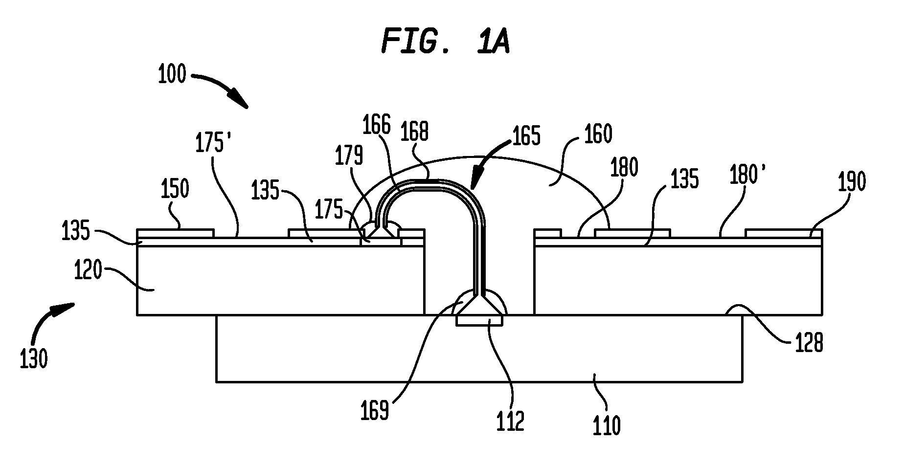
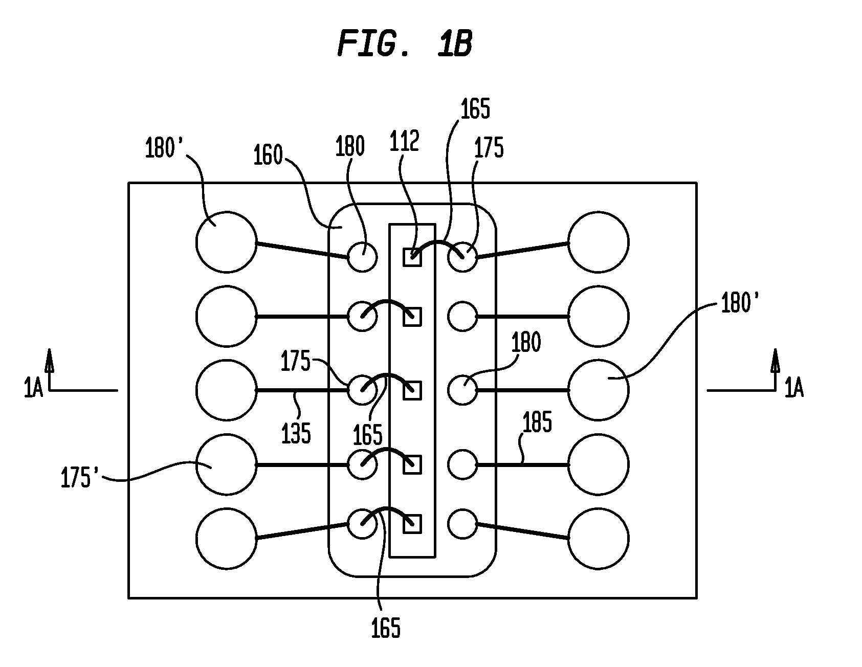
[0055]FIG. 1A shows a sectional view of an example microelectronic assembly 100, according to one embodiment. FIG. 1B is a corresponding plan view from above, in which the view in FIG. 1A is through section line 1A-1A of FIG. 1B. In this example, microelectronic assembly 100 includes a microelectronic device 110 conductively connected to interconnection element 130 through a wire bond 165. The microelectronic assembly 100 differs from conventional arrangements in that it includes a conductor 166 which is insulatively sheathed by an insulative (dielectric) coating 168. Beyond the dielectric coating 168, a conductive encapsulant 160 covers and at least substantially surrounds the wire bond 165. Thus, the conductive encapsulant 160 is disposed at an at least relatively uniform distance (which can be a uniform distance) from the internal conductor 166, such that the conductive encapsulant can act as a reference conductor in a transmission line that includes the central conductor 166 and...
PUM
 Abstract
Description
Claims
Application Information