Low speed, load independent, slew rate controlled output buffer with no DC power consumption

a low speed, load independent, slew rate control technology, applied in pulse manipulation, power consumption reduction, pulse technique, etc., can solve the problems that the data rate of the involved signals may not meet the rise and fall times of the slow edg

Inactive Publication Date: 2011-04-12
SEMICON COMPONENTS IND LLC
View PDF4 Cites 34 Cited by
  • Summary
  • Abstract
  • Description
  • Claims
  • Application Information

AI Technical Summary

Benefits of technology

[0010]The present invention provides a capacitive feedback circuit that substantially reduces, with respect to prior art, slew rate variations when the capacitive load varies substantially.
[0012]Illustratively, the present invention provides for a single inverter input and the charging and discharging of load capacitors and the feedback capacitors through the same output transistor. Current through the feedback capacitor to the gate or control input of the output transistor slows the turn on of the output transistor, reduces the current to the load capacitor thereby slowing the edge rise and fall times of the output voltage. The net effect is to make the slew rate relatively independent of the load capacitors. One way of describing the effect is that the feedback current is dependent upon the load capacitance current. As more load current is delivered, a negative feedback current reduces the rate of increase of load current.
[0013]Illustratively, the present invention employs a combination of PMOS and parallel “native NMOS transistors” as the feedback capacitors. This embodiment provides cleaner output rise and fall times. Herein a “native NMOS transistor” refers to a an NMOS transistor that has not undergone channel doping. Such transistors have lower threshold voltages (usually 0 to 3V, or even negative) because it must rely on the intrinsic background or body of the transistor to set the threshold voltage. Because the threshold voltage is lower, a native device provides a better capacitor with a wider voltage range.

Problems solved by technology

Limitations of the prior art include one nano-second edge times that may generate EMI noise adversely affecting other electronics, and, with large load capacitors, slow edge rise and fall times may not meet the data rates of the signals involved.

Method used


Image

  • Low speed, load independent, slew rate controlled output buffer with no DC power consumption
  • Low speed, load independent, slew rate controlled output buffer with no DC power consumption
  • Low speed, load independent, slew rate controlled output buffer with no DC power consumption

Examples


Embodiment Construction

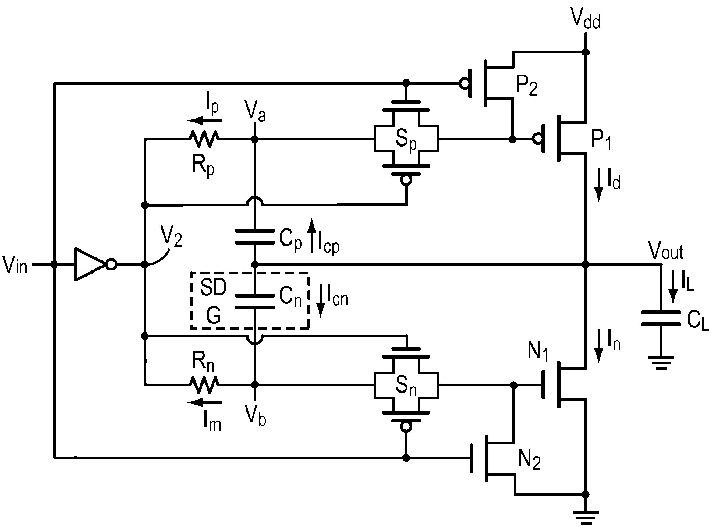
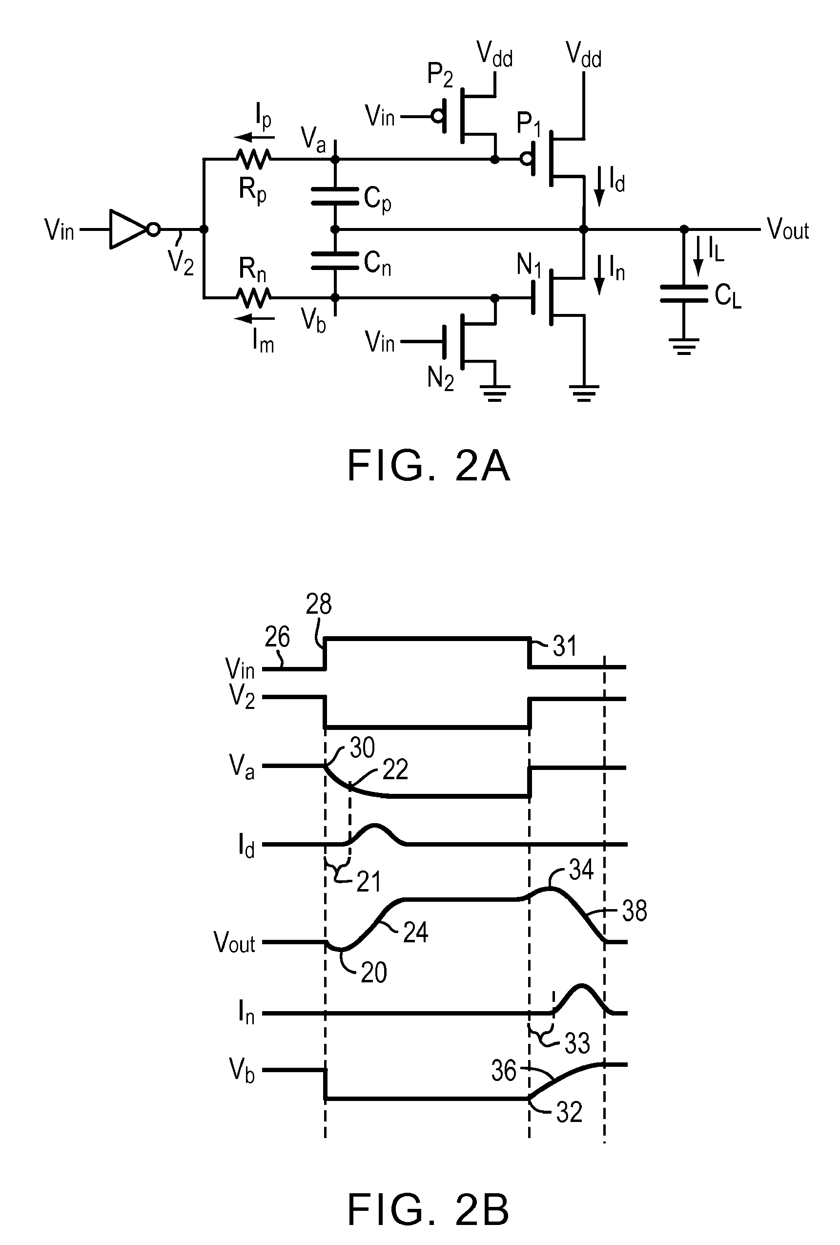
[0023]FIG. 2A is a simplified schematic illustrating a capacitive feedback circuit embodiment of the present invention. FIG. 2B is the associated timing diagram.

[0024]With Vin low 26, V2 is high and P2 on driving Va high and keeping P1 off. Vb is high turning on N1 that drives Vout low. When Vin goes high 28, V2 goes low, and N2 turns on, drives Vb low and turns N1 off. Ip rises drawing current from Cp, Cn and Cl, and Va starts to fall 30. Since P1 is not yet on Id is delayed 21, and Vout falls slightly 20 as some of Ip is taken from Cl.

[0025]Va falls to a point 22 where P1 starts to turn on supplying Id. Id charges Cl and Vout rises 24. As Vout rises some of Id flows through Cp to Va. This feedback action slows the fall of Va, slows the turn on of P1 and the rise if Id. Note that as Vout rises some of Id is diverted through Cn. Nonetheless, Vout rises more slowly but with more control and less dependence on Cl than in prior art buffers. Using other words, the feedback operation ope...


PUM


Abstract

An output buffer utilizes capacitive feedback to control the output slew rate largely independent of load capacitance. The invention slows the rising and falling slew rates and via a capacitance feedback reduces the effect of load capacitance on slew rate, and uses no DC current. Transistor switches are employed to isolate and reduce noise and interaction among the circuit components and functions.

Description

BACKGROUND OF THE INVENTION[0001]1. Field of the Invention[0002]The present invention relates to CMOS output buffers, and more particularly to output buffers with controlled slow slew rates that are relatively independent of capacitive loads and draw no DC power.[0003]2. Background Information[0004]Output buffers must be fast enough to match the high data rates of the signals the buffer is sending, but they must be slow enough to not cause EMI (ElectroMagnetic Interference) with nearby electronics. “Fast enough” and “slow enough” refers to the speed of rising and falling edges. Slew rates,” edge “rise and fall times,” and other such terms as may be used in the art may have different definitions, but they are used interchangeably herein.[0005]Output load capacitance has a substantial effect of slew rates. With a 20 / 1 capacitive load variation, prior art slew rates may vary proportionally or even more depending on the equivalent resistance operating with the load capacitance.[0006]FIG...

Claims


Application Information

Patent Timeline
Patent Type & Authority Patents(United States)
IPC IPC(8): H03K3/00
CPCH03K19/0008H03K19/018521H03K19/00361
Inventor GAGNE, NICKOLE A.BOOMER, JAMES B.YARBROUGH, ROY L.
Owner SEMICON COMPONENTS IND LLC
Why Eureka
Try Eureka