Semiconductor device and method of driving the semiconductor device

a semiconductor and semiconductor technology, applied in the direction of static indicating devices, instruments, transistors, etc., can solve the problems of difficult to make clear distinctions between source and drain, and the tendency to develop dispersion in electrical characteristics

Inactive Publication Date: 2011-04-12
SEMICON ENERGY LAB CO LTD
View PDF37 Cites 30 Cited by
  • Summary
  • Abstract
  • Description
  • Claims
  • Application Information

AI Technical Summary

Benefits of technology

[0420]A structure provided with both advantages, that is a structure in which drops in brightness following deterioration of EL elements are controlled, and one in which correction of dispersion in TFT threshold values is possible, is explained in Embodiment Mode 8 by combining the aforementioned technique with the present invention.

Problems solved by technology

The term TFT as used here refers to a three terminal element having a gate, a source, and a drain, but it is difficult to make clear distinctions between the source and the drain due to the structure of TFTs.
Conversely, TFTs formed by P—Si have a problem in that dispersion in their electrical characteristics tends to develop due to defects in crystal grain boundaries.
This particularly becomes a problem for display devices employing an analog gray scale method.

Method used


Image

  • Semiconductor device and method of driving the semiconductor device
  • Semiconductor device and method of driving the semiconductor device
  • Semiconductor device and method of driving the semiconductor device

Examples


embodiment mode 1

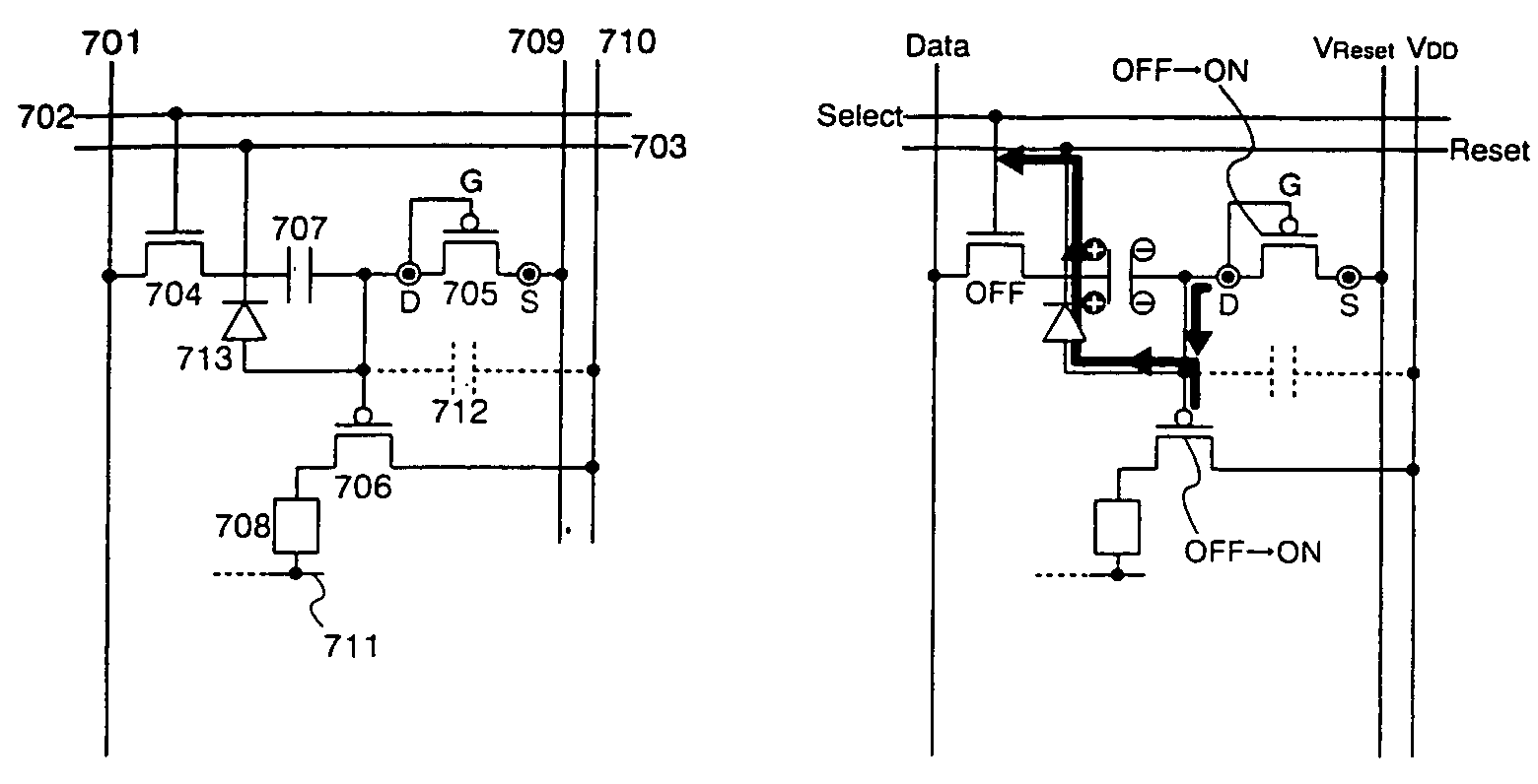
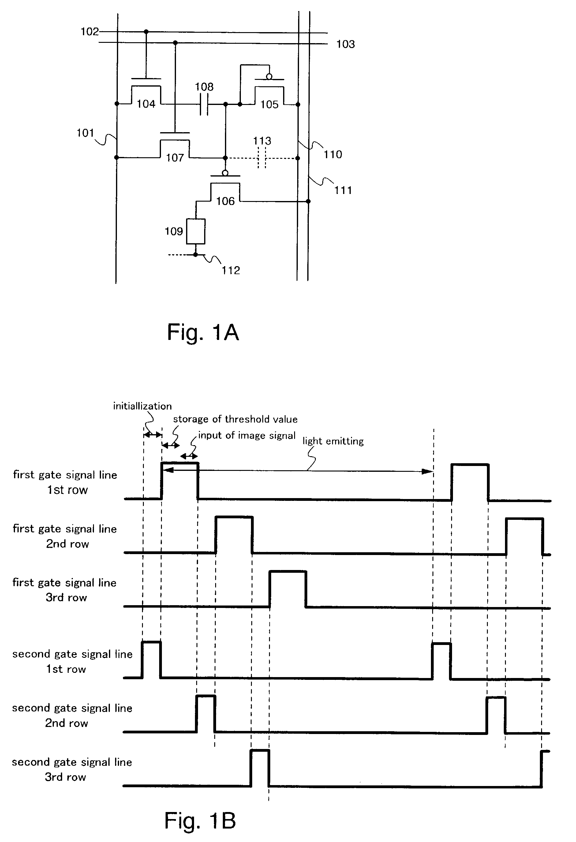
[0375]Embodiment Mode 1 of the present invention is shown in FIG. 1A. Embodiment Mode 1 has a source signal line 101, a first gate signal line 102, a second gate signal line 103, TFTs 104 to 107, capacitor means 108, an EL element 109, a reset electric power source line 110, an electric current supply line 111, and an electric power source line 112. In addition, a storage capacitor means 113 for storing an image signal may also be formed.

[0376]A gate electrode of the TFT 104 is connected to the first gate signal line 102, a first electrode of the TFT 104 is connected to the source signal line 101, and a second electrode of the TFT 104 is connected to a first electrode of the capacitor means 108. A gate electrode and a first electrode of the TFT 105 are connected with each other, and also connected to a second electrode of the capacitor means 108. A second electrode of the TFT 105 is connected to the reset electric power source line 110. A gate electrode of the TFT 106 is connected t...

embodiment mode 2

[0386]A digital gray scale method for controlling the EL element 109 in only two states, one having a brightness of 100% and one a brightness of 0%, by using a region in which it is difficult for TFT threshold values and the like to influence the on electric current is proposed as a method differing from the analog gray scale method discussed above. Only two gray scales, white and black, can be achieved by this method, and therefore multiple gray scales are realized by combining this method with a time gray scale method, a surface area gray scale method, or the like.

[0387]The term time gray scale method refers to a method in which a visible brightness difference can be achieved by utilizing a difference in the amount of time that the EL elements 109 emit light. The operation of this method will be described in detail in another section of this specification, and only two states of the EL elements 109, that is, light emission and non-light emission, need to be used with this type of ...

embodiment mode 3

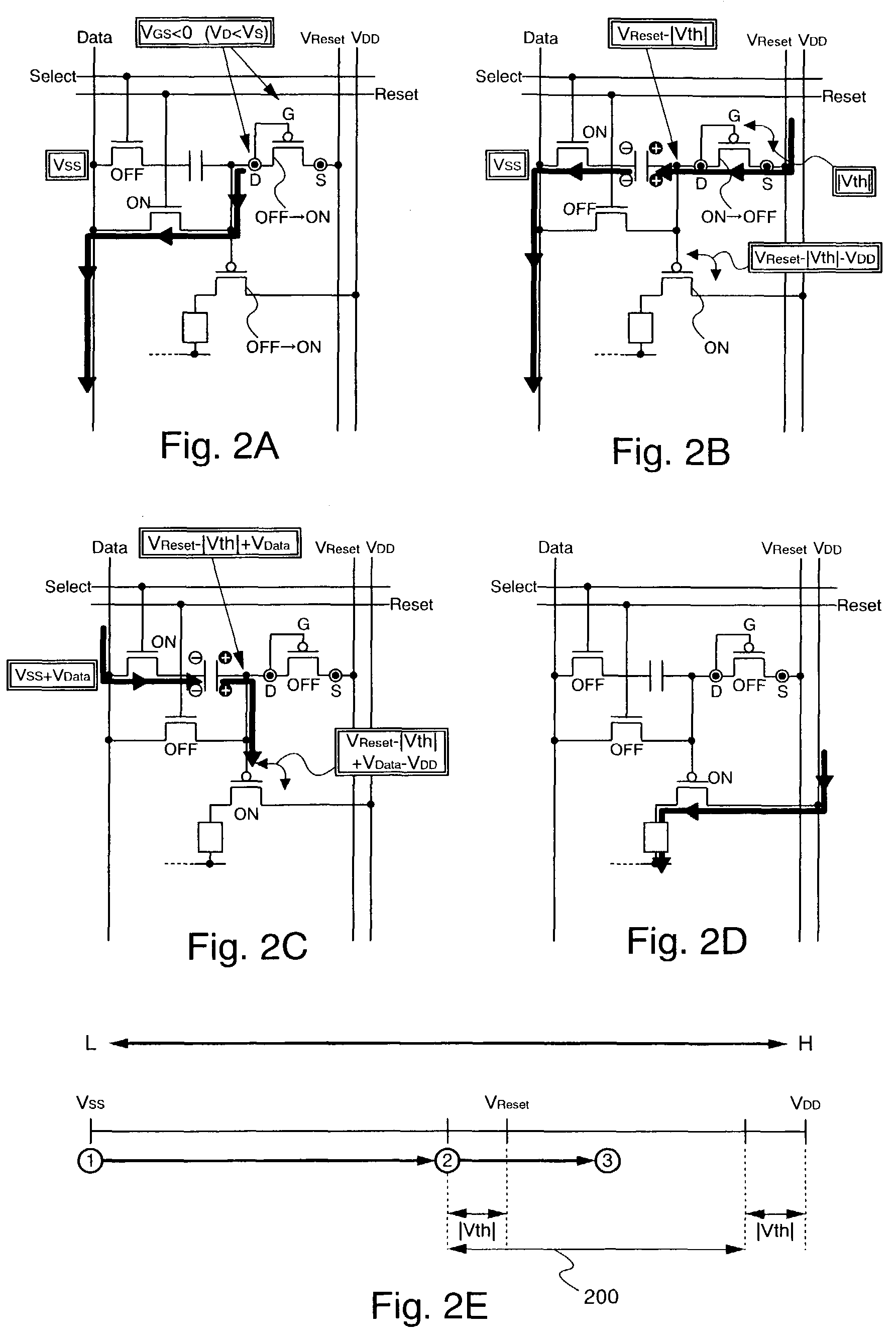
[0389]An example in which some TFT connections differ is shown in FIG. 3A as a third embodiment mode. Although generally similar to the structure shown in FIG. 1A, there is a difference in that a first electrode of a TFT 307 is connected to a second electrode of a TFT 304, not to a source signal line.

[0390]Operation is explained following FIGS. 3B to 3E. The electric potential of a reset electric power source line 310 is VReset, and the electric potential of an electric current supply line 311 is VDD, such that VResetDD. First, the electric potential of a source signal line 301 becomes VSS (where VSSReset), and in addition, first and second gate signal lines 302 and 303 become H level, while TFTs 304 and 307 turn on. The electric potentials of gate electrodes of TFTs 305 and 306 thus drop. The voltage between the gate and the source of the TFT 305 soon becomes lower than the threshold value of the TFT 305, which turns on, and the voltage between the gate and the source of the TFT 30...


PUM


Abstract

Display irregularities in light emitting devices, which develop due to dispersions per pixel in the threshold value of TFTs for supplying electric current to light emitting elements, are obstacles to increasing the image quality of the light emitting devices. An electric potential in which the threshold voltage of a TFT (105) is either added to or subtracted from the electric potential of a reset signal line (110) is stored in capacitor means (108). A voltage, in which the corresponding threshold voltage is added to an image signal, is applied to a gate electrode of a TFT (106). TFTs within a pixel are disposed adjacently, and dispersion in the characteristics of the TFTs does not easily develop. The threshold value of the TFT (105) is thus cancelled, even if the threshold values of the TFTs (106) differ per pixel, and a predetermined drain current can be supplied to an EL element (109).

Description

BACKGROUND OF THE INVENTION[0001]1. Field of the Invention[0002]The present invention relates to a semiconductor device having a transistor and a method of driving the semiconductor device. Further, the present invention relates to an active matrix light emitting device having a semiconductor device with a thin film transistor (hereinafter referred to as a TFT) formed on an insulator such as glass or plastic, and a method of driving the semiconductor device. Also, the present invention relates to electronic equipment using this type of light emitting device.[0003]2. Description of the Related Art[0004]The development of display devices in which light emitting elements such as electro luminescence (EL) elements are used, has become active in recent years. Being self-luminous, the light emitting element is high in visibility and eliminates the need for a backlight that is necessary in liquid crystal display devices (LCDs) etc., thereby being capable of reducing the thickness of such d...

Claims


Application Information

Patent Timeline
Patent Type & Authority Patents(United States)
IPC IPC(8): G09G3/30H01L51/50G09G3/20G09G3/32H01L29/786H05B33/14
CPCG09G3/3648G09G3/3233G09G3/3266G09G3/3283G09G3/3291G09G3/20G09G3/30G09G3/2011G09G2300/0408G09G2300/043G09G2300/0819G09G2300/0842G09G2300/0852G09G2300/0861G09G2310/027G09G2320/0233G09G2320/043G09G3/2022H10K59/131H10K59/1213H10K59/1216G09G3/2077G09G3/3258G09G3/3275G09G2300/0426G09G2310/0286G09G2310/08
Inventor KIMURA, HAJIMETANADA, YOSHIFUMI
Owner SEMICON ENERGY LAB CO LTD
Why Eureka
Try Eureka