Method and system for implementing top down design and verification of an electrical circuit design

a top-down design and circuit technology, applied in the field of top-down design and electrical circuit design verification, can solve the problems of inability of conventional verification tools inability to effectively and efficiently scale upwards to handle very large electronic designs, and inability to handle simulation or formal verification, so as to achieve effective and efficient scaling, increase complexity and the number of transistors, and increase functionality and feature sets

Inactive Publication Date: 2011-05-03
CADENCE DESIGN SYST INC
View PDF4 Cites 23 Cited by
  • Summary
  • Abstract
  • Description
  • Claims
  • Application Information

AI Technical Summary

Benefits of technology

[0005]As the quantity of data in modern IC designs become larger and larger over time, it has become apparent that conventional EDA tools are unable to effectively and efficiently scale upwards to handle very large electronic designs, such as many modern microprocessor, SOC, and systems designs. For example, the ability of conventional verification tools to handle simulation or formal verification is incompatible with many modern IC designs being produced by electronics companies that are constantly increasing in complexity and number of transistors. The basic problem is that conventional simulation and formal verification tools are designed to handle much smaller sets of data than exists for modern designs. This problem is exacerbated for all EDA tools by greatly increased functionality and feature sets for modern IC chips as well as constantly improving IC manufacturing technologies that can create IC chips at ever-smaller feature sizes, which allows increasingly greater quantities of transistors and other objects to be placed within the same chip area.

Problems solved by technology

As the quantity of data in modern IC designs become larger and larger over time, it has become apparent that conventional EDA tools are unable to effectively and efficiently scale upwards to handle very large electronic designs, such as many modern microprocessor, SOC, and systems designs.
For example, the ability of conventional verification tools to handle simulation or formal verification is incompatible with many modern IC designs being produced by electronics companies that are constantly increasing in complexity and number of transistors.
The basic problem is that conventional simulation and formal verification tools are designed to handle much smaller sets of data than exists for modern designs.
The problem with this approach is that the entirety of the design may not be adequately verified and it is ineffective for identifying all problems with the design.
Moreover, this approach may result in design flaws being found much later in the design cycle and even after market / production release of the product.
As is well known in industry, the cost of fixing a design problem tends to significantly increase the further along the product is on the design cycle.
There are many problems with this alternate approach.
For example, the alternate approach fails to provide a consistent relationship across different abstraction levels.
There is a very large gap between what is determined at one level versus what actually happens at another level.
Because of this, this approach requires the verification and correction process at the different levels to be repeated over and over again, often without any assurance that the design problems at a given level are truly being identified.
The problem with conventional transaction based verification tools is that there is no guarantee of relationship between the different abstraction levels.

Method used


Image

  • Method and system for implementing top down design and verification of an electrical circuit design
  • Method and system for implementing top down design and verification of an electrical circuit design
  • Method and system for implementing top down design and verification of an electrical circuit design

Examples


Embodiment Construction

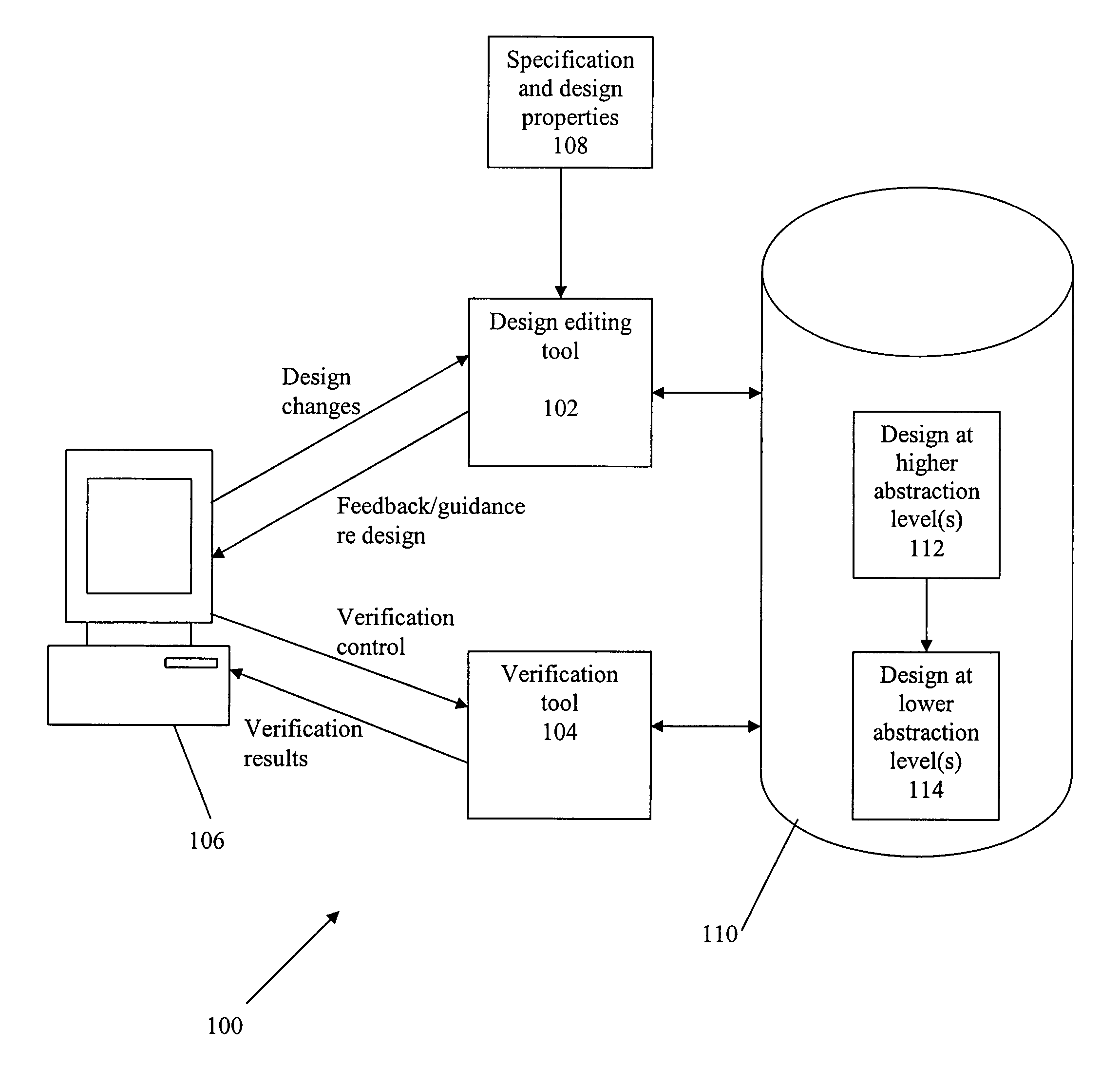
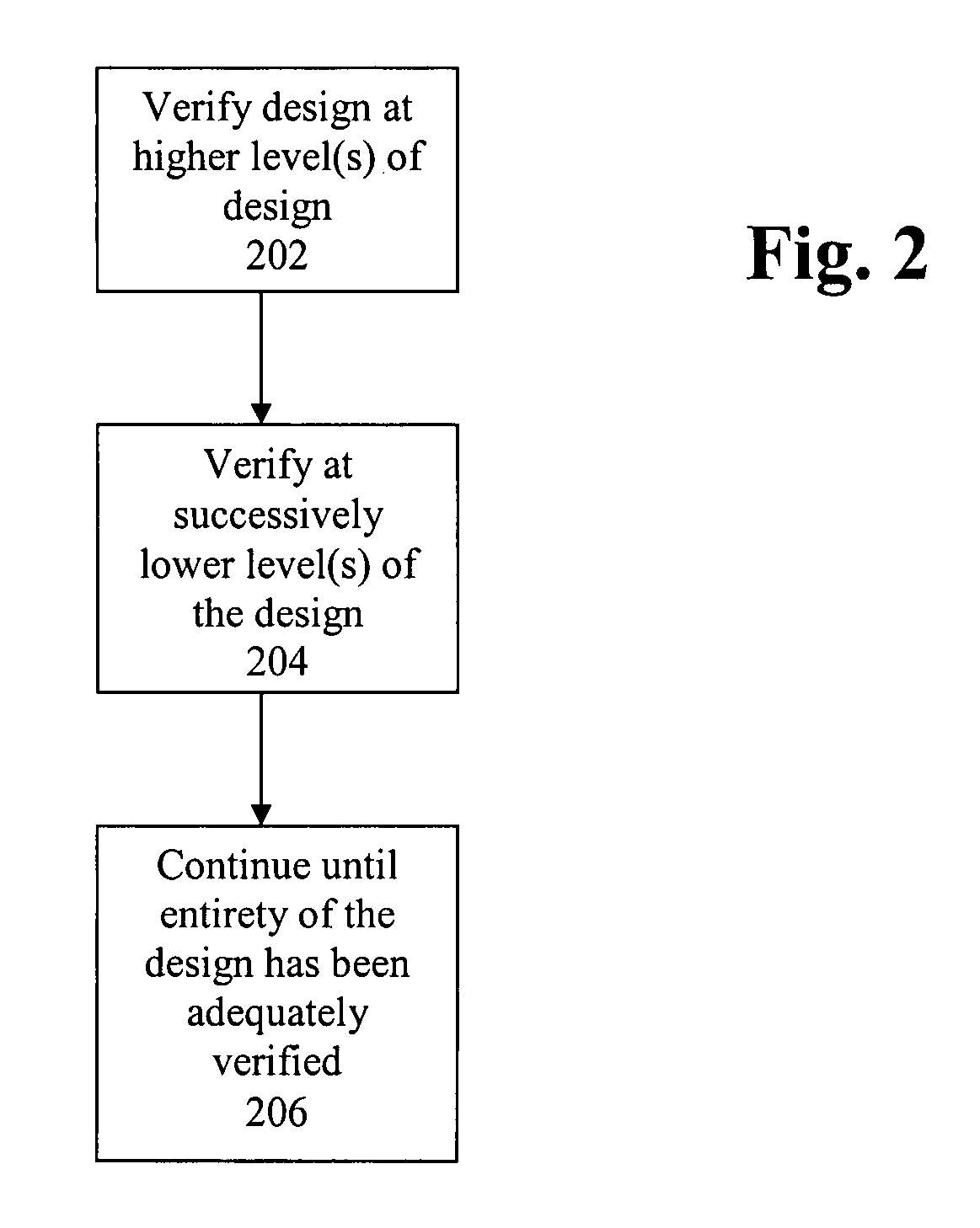
[0017]The present invention provides improved approaches for designing and verifying electronic designs. In some embodiments, design and verification are performed using stepwise refinement techniques, which can also include or be referred to as “top-down” design verification.

[0018]With the present stepwise refinement approach, the electronic design can be acted upon at different levels of abstraction, but with approximately the same level of resolution at each abstraction level. What this means is that the amount of data to be accessed and operated upon at each level of abstraction for the purpose of verification is approximately the same, but the level of detail is different. For example, consider a verification process that first checks an IC design at a high level of abstraction, then at a medium level of abstraction containing more design details, and then at a even lower level of abstraction with many more details. Each level of verification will be performed at approximately ...


PUM


Abstract

Disclosed is a method and system for performing design and verification using stepwise refinement techniques, which can also include or be referred to as “top-down” design verification. With the present stepwise refinement approach, the electronic design can be acted upon at different levels of abstraction, but with approximately the same level of resolution at each abstraction level. A strong relationship of consistency exists between the successive abstraction levels of the design. On account of this consistency, properties that are established or true at one level of the design remain true for all subsequent levels of abstraction of the design.

Description

BACKGROUND AND SUMMARY[0001]Many phases of modern electronic design are performed with computer aided design (CAD) tools or electronic design automation (EDA) systems. To design an integrated circuit, a designer first creates high level behavior descriptions of the IC device using a high-level hardware design language (HDL). Common examples of HDLs include Verilog and VHDL.[0002]An EDA system typically receives the high level behavior descriptions of the IC device and translates this high-level design language into netlists of various levels of abstraction using a computer synthesis process. A netlist describes interconnections of nodes and components on the chip and includes information of circuit primitives such as transistors and diodes, their sizes and interconnections, for example.[0003]An integrated circuit designer may uses a set of layout EDA application programs to create a physical integrated circuit design layout from a logical circuit design. The layout EDA application u...

Claims


Application Information

Patent Timeline
Patent Type & Authority Patents(United States)
IPC IPC(8): G06F17/50
CPCG06F17/504G06F30/3323
Inventor KURSHAN, ROBERT P.MCMILLAN, KENNETH L.
Owner CADENCE DESIGN SYST INC
Why Eureka
Try Eureka