Semiconductor integrated circuit

Active Publication Date: 2011-05-10
INNOLUX CORP
View PDF33 Cites 4 Cited by
  • Summary
  • Abstract
  • Description
  • Claims
  • Application Information

AI Technical Summary

Benefits of technology

[0012]By clamping the potential of the node in the time period when both of the first MOS transistor and the second MOS transistor become non-conducting in the above-described manner, it is possible to prevent characteristic degradation of the MOS transistors due to application of a threshold voltage to the MOS transistors for a long time.
[0037]According to the present invention, transistor characteristic degradation due to application of threshold voltage to MOS transistors for an extended period of time can be prevented because the node potential of the first MOS transistor and the second MOS transistor is clamped in the non-conducting (OFF) time of the first MOS transistor and the second MOS transistor.

Problems solved by technology

Accordingly, a major challenge is to develop a high withstanding voltage circuit that can overcome such technical hurdles or problems encountered in the vertical driving circuit for a LCD.

Method used


Image

  • Semiconductor integrated circuit
  • Semiconductor integrated circuit
  • Semiconductor integrated circuit

Examples


first embodiment

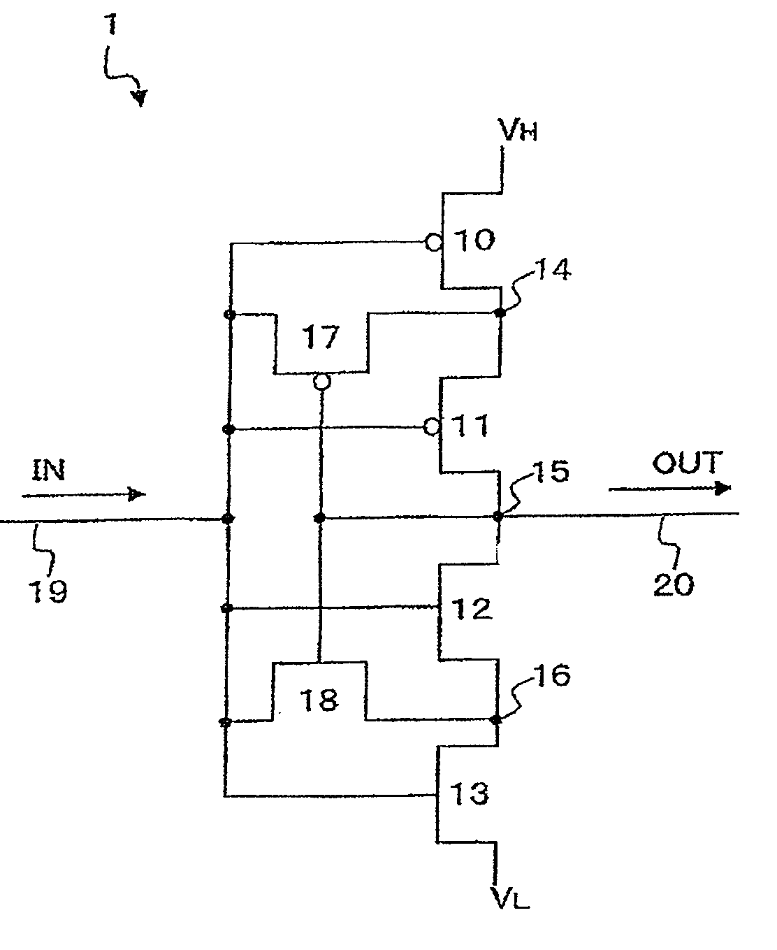
[0044]FIG. 1 is a schematic circuit diagram according to a semiconductor integrated circuit. The circuit as shown in FIG. 1 is an inverter circuit 1 using double gate TFTs (Thin Film Transistors). The inverter circuit 1 includes a series connection of a P-MOS transistor 10, a P-MOS transistor 11, an N-MOS transistor 12 and an N-MOS transistor 13. The P-MOS transistor 10 is connected to a high potential source VH and the N-MOS transistor 13 is connected to a low potential source VL. The gate of each MOS transistor 10˜13 is connected to an input signal line 19. An output signal line 20 is connected to a node of the P-MOS transistor 11 and the N-MOS transistor 12.

[0045]The inverter circuit 1 further includes a P-MOS transistor 17 which connected to a node 14 of the P-MOS transistor 10 and the P-MOS transistor 11 and the input signal line 19, and an N-MOS transistor 18 which connected to a node 16 of the N-MOS transistor 12 and the N-MOS transistor 13 and the input signal line 19. The g...

second embodiment

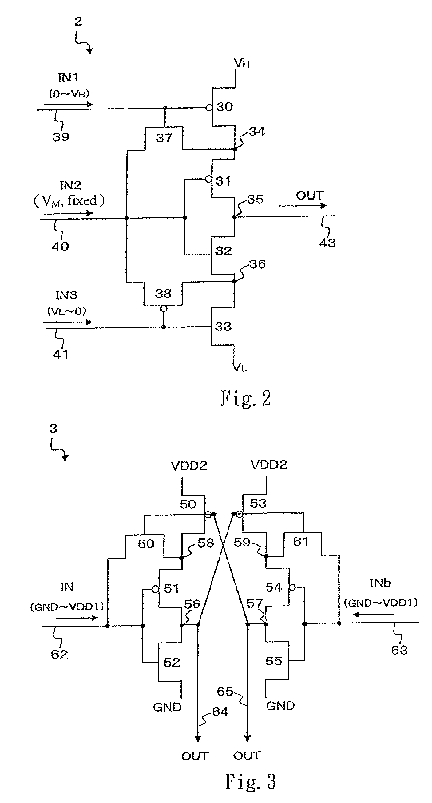
[0049]FIG. 2 is a schematic circuit diagram according to the semiconductor integrated circuit. The circuit as shown in FIG. 2 is a buffer circuit 2. The buffer circuit 2 includes a series connection of a P-MOS transistor 30, a P-MOS transistor 31, an N-MOS transistor 32 and an N-MOS transistor 33. The P-MOS transistor 30 is connected to a high potential source VH and the N-MOS transistor 33 is connected to a low potential source VL. The gate of the P-MOS transistor 30 is connected to a first input signal line 39, the gates of the P-MOS transistor 31 and the N-MOS transistor 32 are connected to a second input signal line 40, and the gate of the N-MOS transistor 33 is connected to a third input signal line 41. An output signal line 43 is connected to a node 35 of the P-MOS transistor 31 and the N-MOS transistor 32.

[0050]The buffer circuit 2 further includes an N-MOS transistor 37 connected between a node 34 of the P-MOS transistors 30, 31 and the second input signal line 40, and a P-M...

third embodiment

[0055]FIG. 3 is a schematic circuit diagram according to the semiconductor integrated circuit. The circuit as shown in FIG. 3 is a level shifter circuit 3. The level shifter circuit 3 is a circuit for providing a voltage range or amplitude GND˜VDD2 from an input signal in the range of GND˜VDD1. In other words, the level shifter circuit 3 performs an amplitude conversion of the potential at the high potential side while clamping the low potential side.

[0056]The level shifter circuit 3 has a series connection of a P-MOS transistor 50, a P-MOS transistor 51 and an N-MOS transistor 52. The P-MOS transistor 50 is connected to a power supply voltage VDD2, while the N-MOS transistor 52 is returned to ground (GND).

[0057]The level shifter circuit 3 further includes a series connection of a P-MOS transistor 53, a P-MOS transistor 54 and an N-MOS transistor 55. The P-MOS transistor 43 is connected to a power supply voltage VDD2, while the N-MOS transistor 55 is returned to ground.

[0058]The gat...


PUM


Abstract

A semiconductor integrated circuit capable of maintaining characteristics of transistors in a circuit including a plurality of cascade connected transistors. The circuit includes an inverter which has a series connection of P-MOS transistors and a pair of N-MOS transistors. The P-MOS transistor is connected to a high potential source VH and the N-MOS transistor is connected to a low potential source VL. The gate of each MOS transistor is connected to an input signal line. The inverter circuit further includes a P-MOS transistor connected between a node and input signal line, and an N-MOS transistor connected between a node of the N-MOS transistors and the input signal line. The gates of the P-MOS transistor and the N-MOS transistor are connected to an output signal line of the inverter circuit.

Description

FIELD OF THE INVENTION[0001]The present invention relates to a semiconductor integrated circuit, and more specifically, to a semiconductor integrated circuit for use as a peripheral driving circuit in a liquid crystal display (LCD).DESCRIPTION OF RELATED ART[0002]In order to miniaturize and reduce production cost for the LCD, developments have been made conventionally for technologies involving placement of integrating peripheral driving circuits on the same substrate as that of a LCD substrate.[0003]The peripheral driving circuits can include a vertical driving circuit for scanning gates of thin film transistors (TFT), and a horizontal driving circuit for supplying a video signal on data bus lines. The peripheral driving circuits are normally fabricated by integrating poly-silicon thin film transistors (p-SiTFT).[0004]Normally, high output voltages in excess of the logic voltage (5 volts or 3.3 volts), are required in a peripheral driving circuit for a LCD. For example, a vertical ...

Claims


Application Information

Patent Timeline
Patent Type & Authority Patents(United States)
IPC IPC(8): H03K19/0175H03K19/094H03L5/00
CPCH03K19/00384H03K19/018528H03K19/018521
Inventor YAMASHITA, KEITARO
Owner INNOLUX CORP
Why Eureka
Try Eureka