Radiation detector

a detector and radiation technology, applied in the field of radiation detectors, can solve problems such as deterioration of sensitivity, and achieve the effects of improving electron transport properties, high electron transport properties, and greatly improving positive hole transport properties

Active Publication Date: 2011-05-24
FUJIFILM CORP
View PDF22 Cites 2 Cited by
  • Summary
  • Abstract
  • Description
  • Claims
  • Application Information

AI Technical Summary

Benefits of technology

[0021]The radiation detector of the present invention comprises the recording photoconductive layer and the electrodes provided on both sides of the recording photoconductive layer. In the radiation detector of the present invention, electric charges, which are generated within the recording photoconductive layer when radiation is irradiated thereon while a predetermined biasing voltage is being applied between the electrodes, are read out as electric signals. The recording photoconductive layer is formed by amorphous selenium that contains alkali metal elements within a range from 0.0007 atomic ppm to 0.0035 atomic ppm. Therefore, the positive hole transport properties can be greatly improved while maintaining high electron transport properties. The electron transport properties are improved over pure selenium, which is said to have great fluctuations in electron transport properties, and further, the positive hole transport properties are improved, resulting in a radiation detector which is superior in charge transport properties.
[0022]In addition, it is preferable for the recording photoconductive layer to be doped with As, which has a crystallization preventing function. This is because the crystallization temperature of pure selenium and selenium doped with alkali metals is low, these materials crystallize easily, and the cores of crystallization are often generated during vapor deposition. A radiation detector which is superior in durability can be obtained, by causing the recording photoconductive layer to further contain As within a range from 0.1 atomic % to 0.5 atomic %, or by providing a layer formed by amorphous selenium adjacent to the recording photoconductive layer at least one side thereof, having a thickness within a range from 0.2 μm to 2 μm and containing As within a range from 2 atomic % to 14 atomic %.

Problems solved by technology

However, there is a trend for many structural faults to be included therein due to the amorphous nature of a-Se, which leads to deterioration of sensitivity.

Method used


Image

  • Radiation detector
  • Radiation detector
  • Radiation detector

Examples


first embodiment

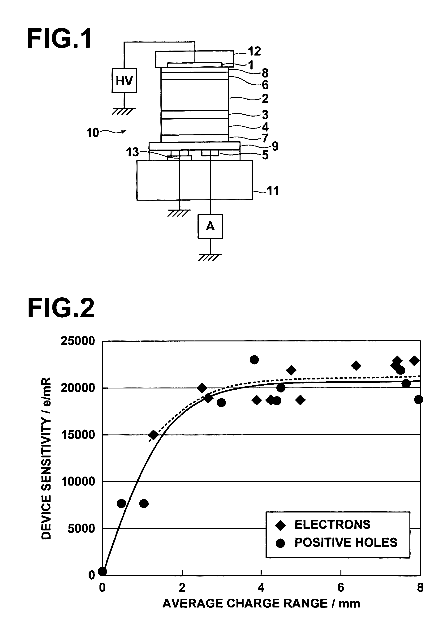
[0034]Hereinafter, a radiation detector that employs the optical readout method will be described. FIG. 1 is a sectional diagram that illustrates the schematic construction of a radiation detector 10 according to the present invention.

[0035]The radiation detector 10 comprises: an upper electrode 1 which is transmissive with respect to recording radiation; a recording photoconductive layer 2 that exhibits conductivity when irradiated by the radiation transmitted through the upper electrode 1; a charge accumulating layer 3 that functions substantially as an insulator with respect to charges which are charged at the upper electrode 1 (latent image polarity charges: negative electric charges, for example) and functions substantially as a conductor with respect to electric charges of the opposite polarity (transport polarity charges: in the case described above, positive electric charges); a readout photoconductive layer 4 that exhibits conductivity when irradiated by readout light; and ...

second embodiment

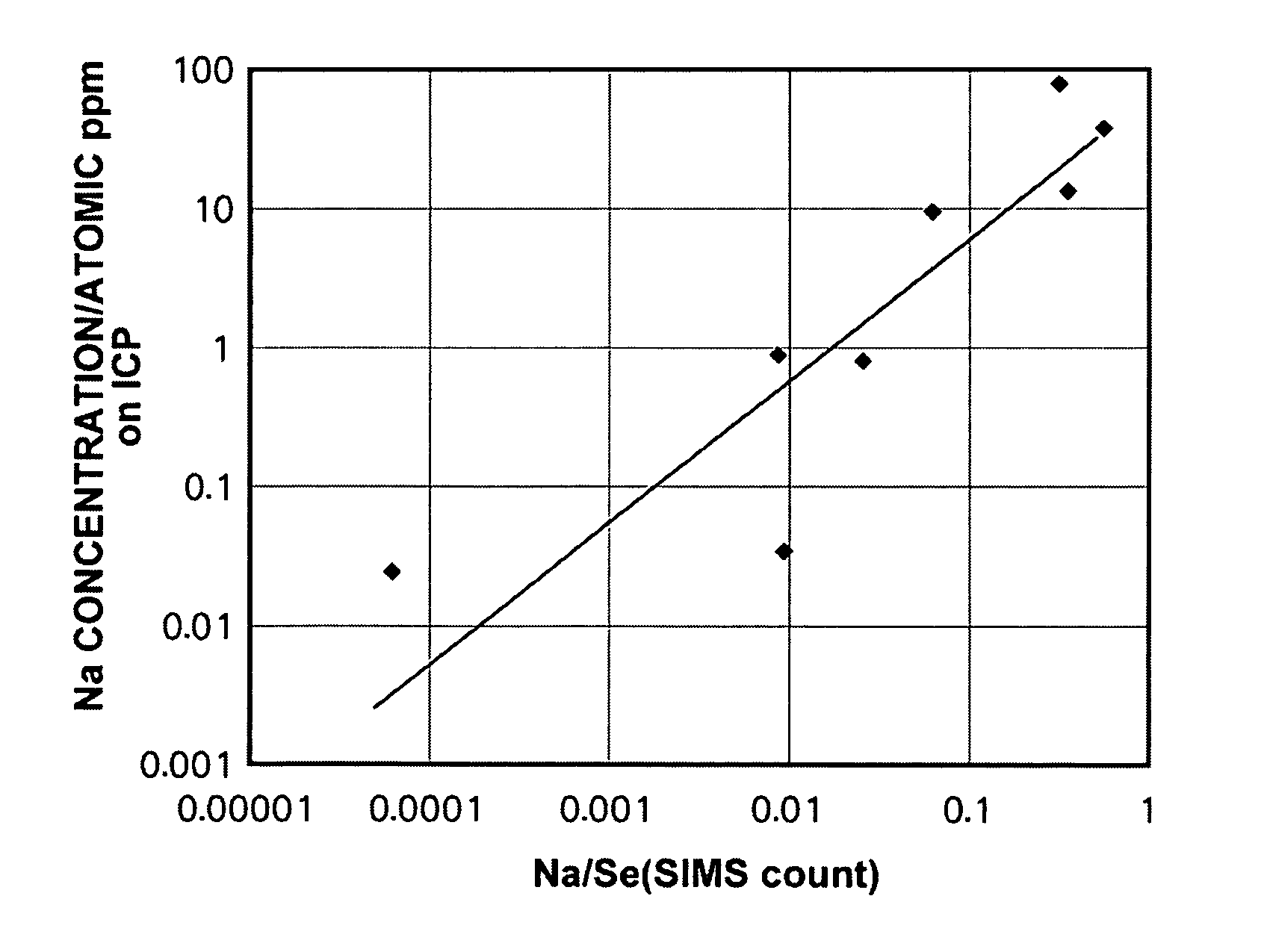
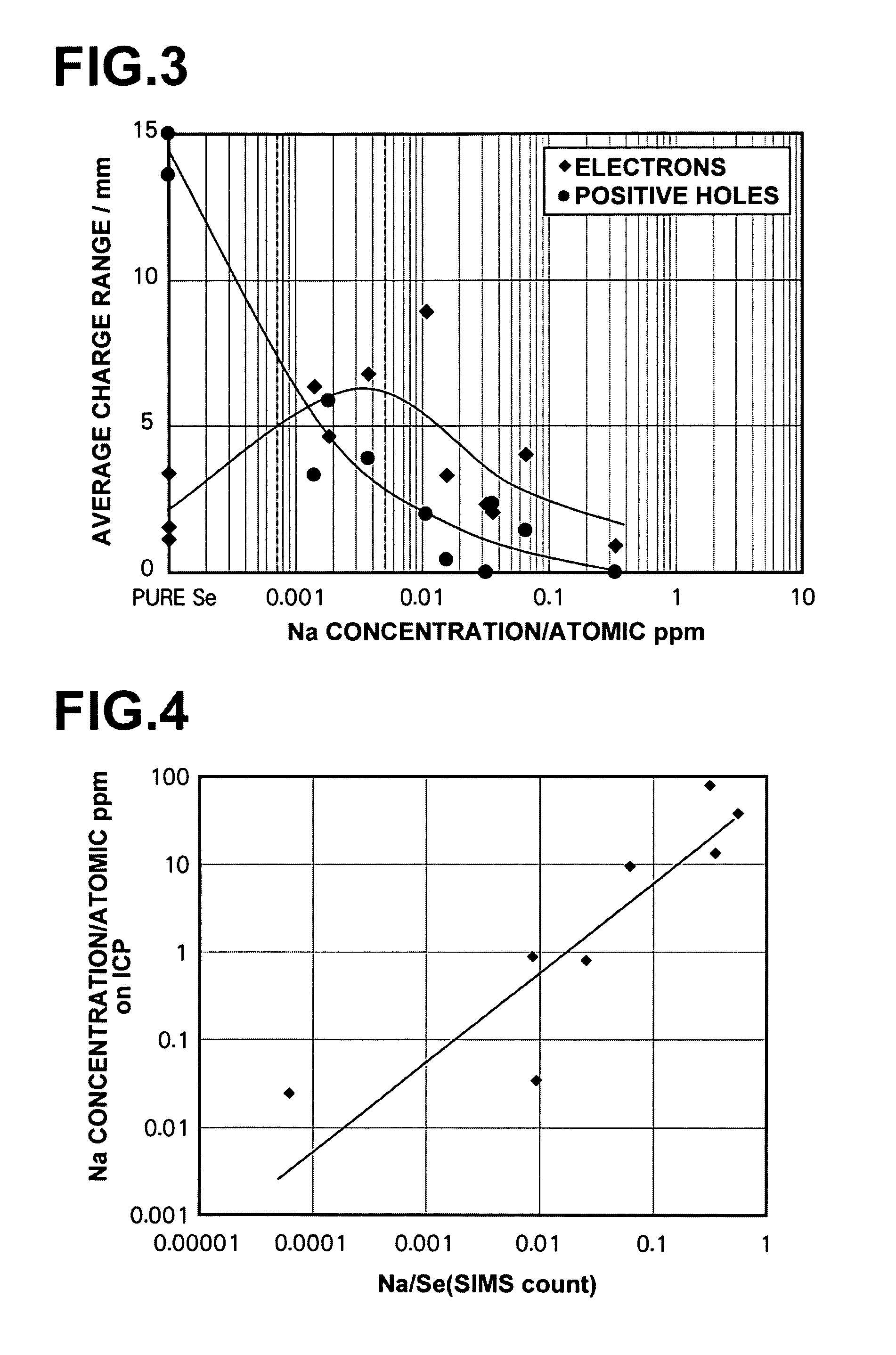
[0055]FIG. 9 is a schematic sectional view that illustrates the structure of a radiation detector according to the present invention. In FIG. 9, elements which are the same as those illustrated in FIG. 1 are denoted with the same reference numerals, and detailed descriptions thereof will be omitted insofar as they are not particularly necessary. In the radiation detector 10 illustrated in FIG. 9, a layer 15 (hereinafter, referred to as “adjacent layer 15”) formed by amorphous selenium, having a thickness within a range from 0.2 μm to 2 μm and containing As within a range from 2 atomic % to 14 atomic %, is provided adjacent to the recording photoconductive layer 2 at one side thereof. Crystal cores are likely to be generated particularly at the interface of the recording photoconductive layer 2 at which the adjacent layer 15 is positioned. This is due to various factors, such as: amorphous layers are likely to be unstable at interfaces from a free energy viewpoint; the possibility th...


PUM

PropertyMeasurementUnit
thicknessaaaaaaaaaa
thicknessaaaaaaaaaa
thicknessaaaaaaaaaa

Abstract

A radiation detector is constituted by: a recording photoconductive layer; and electrodes provided on both sides of the photoconductive layer. Electric charges, which are generated within the recording photoconductive layer when radiation is irradiated thereon while a predetermined biasing voltage is being applied between the electrodes, are read out as electric signals. The recording photoconductive layer is formed by amorphous selenium that contains alkali metal elements within a range from 0.0007 atomic ppm to 0.0035 atomic ppm.

Description

CROSS-REFERENCE TO RELATED APPLICATION[0001]This application claims the benefit of Japanese Patent Application 136631 / 2008, filed May 29, 2008, the disclosure of which is incorporated herein by reference in its entirety.BACKGROUND OF THE INVENTION[0002]1. Field of the Invention[0003]The present invention is related to a radiation detector which is suited to application to radiation imaging apparatuses, such as X-ray imaging apparatuses.[0004]2. Description of the Related Art[0005]Currently, various X-ray imaging apparatuses that employ solid state radiation detectors (having semiconductors as the main portions thereof) as X-ray image information recording means have been proposed and are in practical use in the field of X-ray (radiation) imaging for the purposes of medical diagnosis and the like.[0006]Various types of radiation detectors to be employed by the X-ray imaging apparatuses have been proposed. From the viewpoint of a charge generating process for converting X-rays to elec...

Claims


Application Information

Patent Timeline
Patent Type & Authority Patents(United States)
IPC IPC(8): G03C5/16
CPCG01T1/246G01T1/244
Inventor IRISAWA, KAKUNODA, KAZUHIROHAYASHI, KENICHIYAMANE, KATSUTOSHIMIYAKE, KIYOTERU
Owner FUJIFILM CORP
Why Eureka
Try Eureka