High efficiency light emitting diode (LED)

a light emitting diode and high-efficiency technology, applied in the direction of planar/plate-like light guides, light guides for lighting systems, lighting and heating apparatus, etc., can solve the problems of difficult surface feature shaping for improving light extraction efficiency, requiring zno crystal growth equipment, and difficult to grow thick layers, etc., to reduce light absorption, and increase the efficiency of led

Inactive Publication Date: 2011-06-07
RGT UNIV OF CALIFORNIA
View PDF31 Cites 15 Cited by
  • Summary
  • Abstract
  • Description
  • Claims
  • Application Information

AI Technical Summary

Benefits of technology

[0023]Another embodiment of the present invention is a Light Emitting Diode assembly. Such an assembly in accordance with the present invention comprises a substrate, a light emitting device, comprising an n-type Group III nitride layer coupled to the substrate, an active layer, coupled to the n-type Group III nitride layer, wherein the active layer emits light in at least a first wavelength region, and a p-type Group III nitride layer, coupled to the active layer, at least one oxide layer, coupled to the light emitting device, the at least one oxide layer being shaped into a form that increases the efficiency of the light emitting device by reducing light absorption in the light emitting device, an optical element, coupled to the at least one oxide layer, and a phosphor, optically coupled to the at least one oxide layer, wherein light in at least the first wavelength region emitted by the light emitting device passes through the phosphor and excites the phosphor to emit light in at least a second wavelength region.
[0024]Another embodiment of the present invention is a Light Emitting Diode (LED) emitting multiple wavelength regions of light, which comprises an active Group III nitride layer, wherein the active Group III nitride layer emits light in at least a first wavelength region, at least one oxide layer, coupled to the light emitting device, wherein the at least one oxide layer is substantially transparent in the first wavelength region, the at least one oxide layer being shaped into a form that increases the efficiency of the LED by reducing light absorption in the LED, and a phosphor, optically coupled to the at least one oxide layer such that light in at least the first wavelength region strikes the phosphor and excites the phosphor to emit light in at least a second wavelength region, such that light in at least the first wavelength region and the second wavelength region are emitted by the LED.
[0025]Such an embodiment further optionally includes a lens, coupled between the oxide layer and the phosphor, wherein the lens increases the efficiency of the LED by reducing light absorption in the LED.

Problems solved by technology

Also, surface feature shaping for improving light extraction efficiency is difficult because of the hardness of GaN material and the instability of p-type GaN conductivity.
However, this method requires ZnO crystal growth equipment, which uses ultra-high vacuum conditions.
Moreover, it is difficult to grow thick layers, e.g., 500 μm thick layers, that are suitable for feature shaping for the purpose of light extraction.

Method used


Image

  • High efficiency light emitting diode (LED)
  • High efficiency light emitting diode (LED)
  • High efficiency light emitting diode (LED)

Examples


Embodiment Construction

[0044]In the following description of the preferred embodiment, reference is made to the accompanying drawings which form a part hereof, and in which is shown by way of illustration a specific embodiment in which the invention may be practiced. It is to be understood that other embodiments may be utilized and structural changes may be made without departing from the scope of the present invention.

[0045]Overview

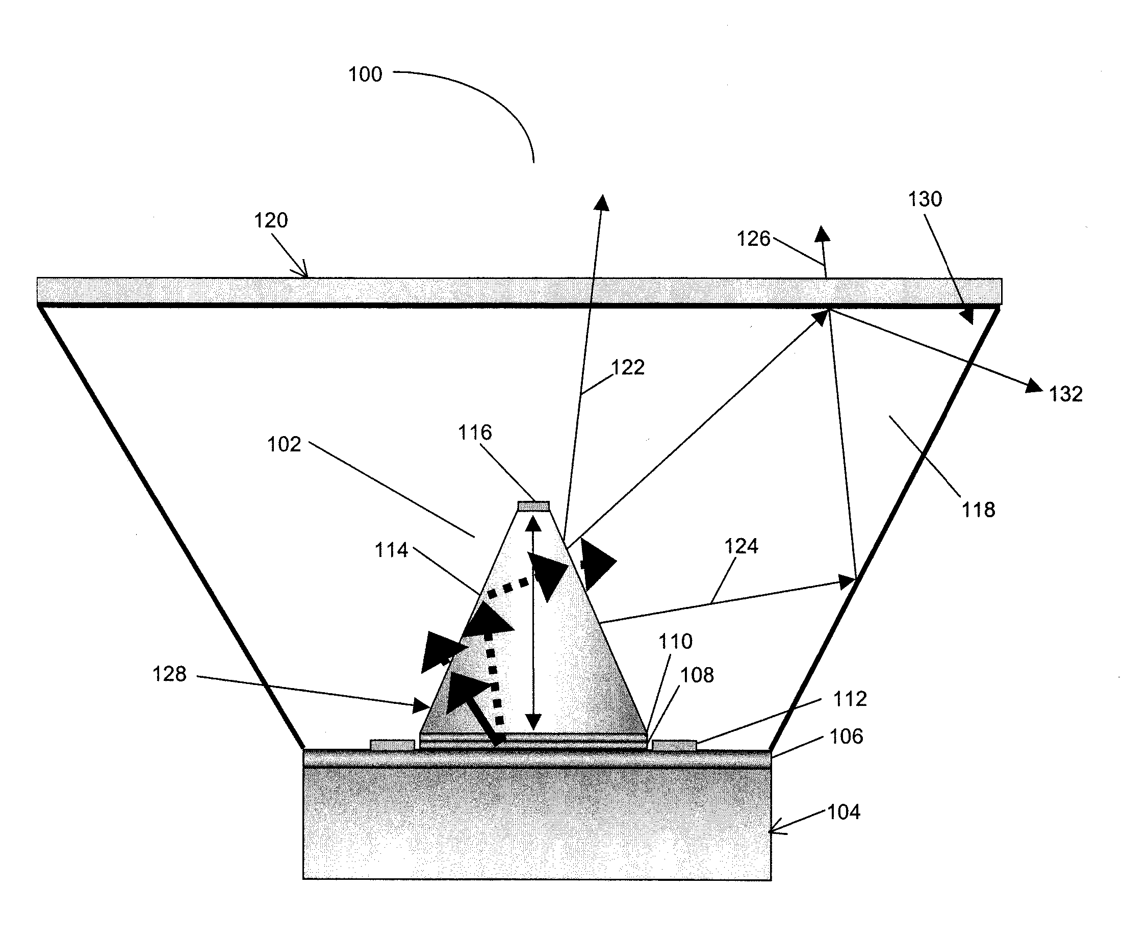
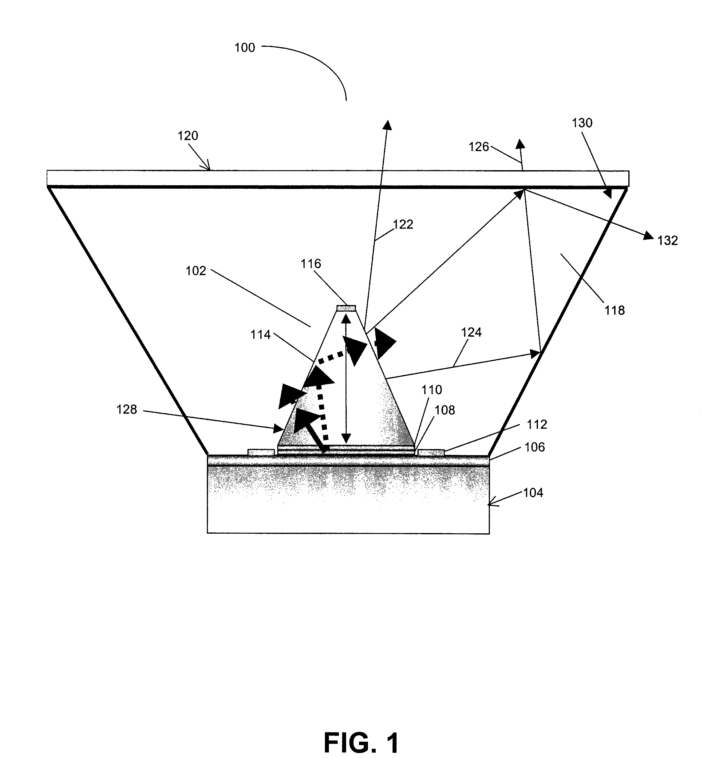
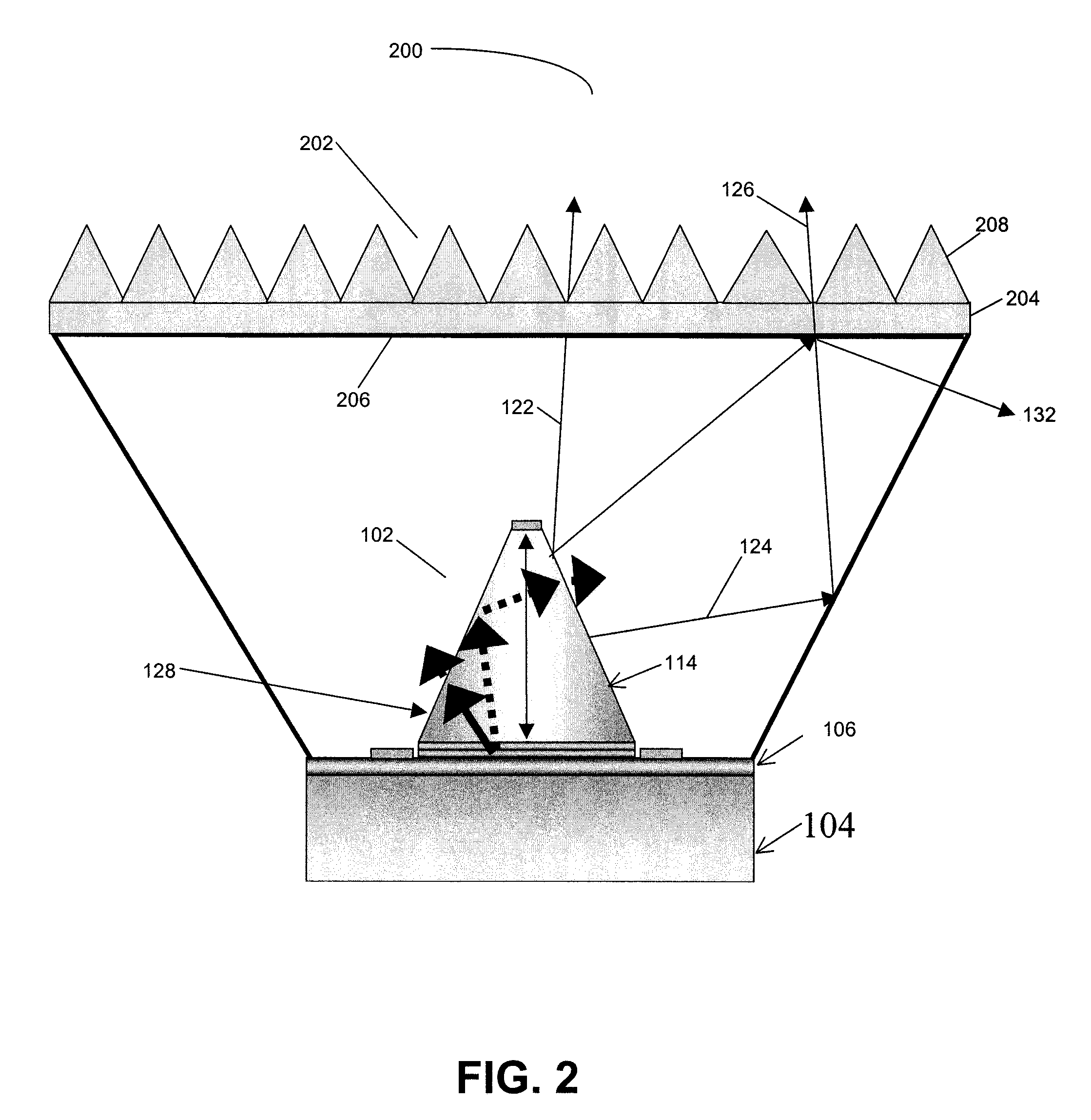
[0046]The purpose of the present invention is to provide a means of increasing the light extraction efficiency from a light emitting diode (LED) by combining shaped high refractive index elements with an (Al, Ga, In)N LED and shaped optical elements. By increasing light transmittance and light extraction, subsequent device performance is increased.

[0047]In one embodiment of the present invention, a high refractive index ZnO layer is wafer bonded to a GaN LED. A cone is etched in the high refractive index ZnO layer and contacts are fabricated on the GaN LED. The ZnO / GaN hybrid ...


PUM


Abstract

An (Al, Ga, In)N light emitting diode (LED), wherein light extraction from chip and / or phosphor conversion layer is optimized. By novel shaping of LED and package optics, a high efficiency light emitting diode is achieved.

Description

CROSS-REFERENCE TO RELATED APPLICATIONS[0001]This application is related to the following co-pending and commonly-assigned applications:[0002]U.S. Provisional Application Ser. No. 60 / 691,710, filed on Jun. 17, 2005, by Akihiko Murai, Christina Ye Chen, Lee S. McCarthy, Steven P. DenBaars, Shuji Nakamura, and Umesh K. Mishra, entitled “(Al, Ga, In)N AND ZnO DIRECT WAFER BONDING STRUCTURE FOR OPTOELECTRONIC APPLICATIONS AND ITS FABRICATION METHOD,”;[0003]U.S. Provisional Application Ser. No. 60 / 732,319, filed on Nov. 1, 2005, by Akihiko Murai, Christina Ye Chen, Daniel B. Thompson, Lee McCarthy, Steven P. DenBaars, Shuji Nakamura, and Umesh K. Mishra, entitled “(Al, Ga, In)N AND ZnO DIRECT WAFER BONDED STRUCTURE FOR OPTOELECTRONIC APPLICATIONS, AND ITS FABRICATION METHOD,”;[0004]U.S. Provisional Application Ser. No. 60 / 764,881, filed on Feb. 3, 2006, by Akihiko Murai, Christina Ye Chen, Daniel B. Thompson, Lee S. McCarthy, Steven P. DenBaars, Shuji Nakamura, and Umesh K. Mishra, entit...

Claims


Application Information

Patent Timeline
Patent Type & Authority Patents(United States)
IPC IPC(8): H01L33/38F21K99/00H01L33/20H01L33/50H01L33/58H01L33/60
CPCH01L33/20H01L33/507H01L33/60H01L33/58H01L33/508G02B6/0018H01L2933/0091
Inventor DENBAARS, STEVEN P.NAKAMURA, SHUJISPECK, JAMES S.
Owner RGT UNIV OF CALIFORNIA
Why Eureka
Try Eureka